Ram Koganti (rkoganti@ichips.intel.com)
Khader Mohammad (kmohamm@ichips.intel.com)
This report describes the implementation of a digital circuit that computes the Greatest Common Divisor (GCD) of two unsigned eight-bit integers. Two implementations are presented here, one optimized for area and the other optimized for speed. Though the high level architecture is the same, the subcircuits are different, resulting in two different designs.
This report is organized as follows. First we describe the black-box behavior of the entity. In section 2, we present an architecture of the GCD circuit. The GCD circuit is designed using a top-down aproach, and in section 3 we describe the sub-circuits used. The different sub-circuits result in different designs of the GCD logic. In Section 4, we compares the Area/Performance Tradeoffs for both the implementations. In Section 5, we present out validation methodology and describe the architecture of the test benches. In Section 6 we present some simulation results.
Figure 1 shows the GCD entity.

Figure 1: Greatest Common Divisor Component (For a Printable figure click here)
Two 8-bit unsigned integers are placed on the NUM1[7:0] and NUM2[7:0] data buses. Then, the GCD computation is triggered by enabling the START signal. Once the GCD computation is completed the GCDValid signal goes high and the GCD[7:0] data bus should be sampled to obtain the Greates Common Divisor of the two input numbers. Note that once GCD computation has started, a new calculation cannot be started until the GCValid signal goes high or the System is reset by pulling up the Reset signal.
The circuit implements the following well known algorithm for computing the GCD.
while ((num1 != 0) && (num2 != 0))
{
}; if (num1 == 0) gcd = num2; if (num2 == 0) gcd = num1; |
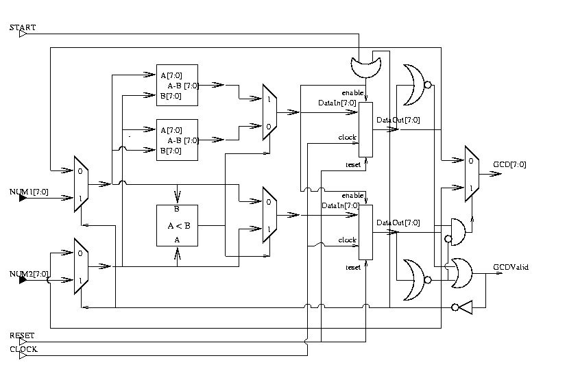
Figure 2 shows the schematic for the GCD circuit.

Figure 2: GCD Cicuit Schematic
(For a Printable figure click here)
The datapath consists of two registers, two subtractors and 5 multiplexers. The registers effectively store the result of the GCD computation for one loop. Once a register contains a zero, GCD computation is stopped, and the numeric in the other Register is output as the GCD. The first two multiplexers are used to load new input values or recycle register values. The next two multiplexers are used to select the appropriate value to load into the register depending on which number is greater. The final multiplexer choses the output from the two registers.
Table 1 summarizes the entities in the datapath.
| Entity | Number |
| Registers | 2 |
| Comparators | 1 |
| Subtractors | 2 |
| Multiplexers | 5 |
The control logic does four things
The implementation makes use of the following sub-circuits. The Subtractor subcircuit has two architectures, one optimized for speed and the other optimized for Area/Power. This results in two different implementations of the GCD Circuit.
The multiplexer circuit is a simple 2 level AND-OR network. The VHDL code for the mulitplexer is shown in Figure 3.
| --------------------------------------- -- 8-bit 1-select multiplexer -- This multiplexer is used to chose -- one of two 8-bit integers --------------------------------------- entity mux8_2 is port( D0, D1: in bit_vector(7 downto 0); S: in bit; Dat: out bit_vector(7 downto 0)); end mux8_2; architecture structural of mux8_2 is begin g1: FOR i IN 0 TO 7 GENERATE Dat(i) <= (D1(i) AND S) OR (D0(i) AND (NOT S)); END GENERATE; end structural; |
Figure 3: Multiplexer Code
There are two implementations of the subtractor circuit. One uses the carry lookahead adder, where as the other uses a ripple-carry adder. The subtractor uses 2's complement representation for the minuend. The input carry bit to the 8-bit adder is always set to 1 and the constant propogated. This can be done because the magnitude comparator is used to select the correct subtraction from the 2 subtractor circuits. The VHDL code for the carry look-ahead subtractor is shown in Figure 4.
| ---------------------------------------- -- 8-bit subtractor (A-B) -- uses a carry lookahead adder -- and 2's complement ---------------------------------------- entity AminusB is port ( A, B: in bit_vector(7 downto 0); AminusB: out bit_vector(7 downto 0)); end AminusB; architecture structural of AminusB is signal Bcompl, P, G, C: bit_vector(7 downto 0); begin Bcompl <= NOT B; P <= A XOR Bcompl; G <= A AND Bcompl; C(0) <= '1'; g1: FOR i IN 0 TO 7 GENERATE AminusB(i) <= P(i) XOR C(i); END GENERATE; C(1) <= G(0) OR (P(0)); C(2) <= G(1) OR (P(1) AND G(0)) OR (P(1) AND P(0)); C(3) <= G(2) OR (P(2) AND G(1)) OR (P(2) AND P(1) AND G(0)) OR (P(2) AND P(1) AND P(0)); C(4) <= G(3) OR (P(3) AND G(2)) OR (P(3) AND P(2) AND G(1)) OR (P(3) AND P(2) AND P(1) AND G(0)) OR (P(3) AND P(2) AND P(1) AND P(0)); C(5) <= G(4) OR (P(4) AND G(3)) OR (P(4) AND P(3) AND G(2)) OR (P(4) AND P(3) AND P(2) AND G(1)) OR (P(4) AND P(3) AND P(2) AND P(1) AND G(0)) OR (P(4) AND P(3) AND P(2) AND P(1) AND P(0)); C(6) <= G(5) OR (P(5) AND G(4)) OR (P(5) AND P(4) AND G(3)) OR (P(5) AND P(4) AND P(3) AND G(2)) OR (P(5) AND P(4) AND P(3) AND P(2) AND G(1)) OR (P(5) AND P(4) AND P(3) AND P(2) AND P(1) AND G(0)) OR (P(5) AND P(4) AND P(3) AND P(2) AND P(1) AND P(0)); C(7) <= G(6) OR (P(6) AND G(5)) OR (P(6) AND P(5) AND G(4)) OR (P(6) AND P(5) AND P(4) AND G(3)) OR (P(6) AND P(5) AND P(4) AND P(3) AND G(2)) OR (P(6) AND P(5) AND P(4) AND P(3) AND P(2) AND G(1)) OR (P(6) AND P(5) AND P(4) AND P(3) AND P(2) AND P(1) AND G(0)) OR (P(6) AND P(5) AND P(4) AND P(3) AND P(2) AND P(1) AND P(0)); end structural; |
Figure 4: carry-lookahead subtractor VHDL code
The code for the ripple-carry subtractor is shown in Figure 5.
| ---------------------------------------- -- subtractor circuit optimized for area ---------------------------------------- architecture Area_Optimized of AminusB is signal Bcompl, P, G, C: bit_vector(7 downto 0); begin Bcompl <= NOT B; P <= A XOR Bcompl; G <= A AND Bcompl; C(0) <= '1'; g1: FOR i IN 0 TO 7 GENERATE AminusB(i) <= P(i) XOR C(i); END GENERATE; g2: FOR i IN 1 TO 7 GENERATE C(i) <= G(i-1) OR (P(i-1) AND C(i-1)); END GENERATE; end Area_Optimized; |
Figure 5: ripple-carry subtractor VHDL code
The structural vhdl code for the comparator is shown in Figure 6.
| ---------------------------------------- -- AcomB comparator -- 8-bit A > B, A = B and A < B -- comparator implemented using -- standard gates ---------------------------------------- entity AcomB is port( A,B: in bit_vector(7 downto 0); AgtB: out bit; AeqB: out bit; AltB: out bit); end AcomB; architecture structural of AcomB is signal AxnorB: bit_vector(7 downto 0); begin AxnorB <= NOT (A xor B); AeqB <= AxnorB(0) AND AxnorB(1) AND AxnorB(2) AND AxnorB(3) AND AxnorB(4) AND AxnorB(5) AND AxnorB(6) AND AxnorB(7); AgtB <= (A(7) AND NOT B(7)) OR (AxnorB(7) AND A(6) AND NOT B(6)) OR (AxnorB(7) AND AxnorB(6) AND A(5) AND NOT B(5)) OR (AxnorB(7) AND AxnorB(6) AND AxnorB(5) AND A(4) AND NOT B(4)) OR (AxnorB(7) AND AxnorB(6) AND AxnorB(5) AND AxnorB(4) AND A(3) AND NOT B(3)) OR (AxnorB(7) AND AxnorB(6) AND AxnorB(5) AND AxnorB(4) AND AxnorB(3) AND A(2) AND NOT B(2)) OR (AxnorB(7) AND AxnorB(6) AND AxnorB(5) AND AxnorB(4) AND AxnorB(3) AND AxnorB(2) AND A(1) AND NOT B(1)) OR (AxnorB(7) AND AxnorB(6) AND AxnorB(5) AND AxnorB(4) AND AxnorB(3) AND AxnorB(2) AND AxnorB(1) AND A(0) AND NOT B(0)); AltB <= (B(7) AND NOT A(7)) OR (AxnorB(7) AND B(6) AND NOT A(6)) OR (AxnorB(7) AND AxnorB(6) AND B(5) AND NOT A(5)) OR (AxnorB(7) AND AxnorB(6) AND AxnorB(5) AND B(4) AND NOT A(4)) OR (AxnorB(7) AND AxnorB(6) AND AxnorB(5) AND AxnorB(4) AND B(3) AND NOT A(3)) OR (AxnorB(7) AND AxnorB(6) AND AxnorB(5) AND AxnorB(4) AND AxnorB(3) AND B(2) AND NOT A(2)) OR (AxnorB(7) AND AxnorB(6) AND AxnorB(5) AND AxnorB(4) AND AxnorB(3) AND AxnorB(2) AND B(1) AND NOT A(1)) OR (AxnorB(7) AND AxnorB(6) AND AxnorB(5) AND AxnorB(4) AND AxnorB(3) AND AxnorB(2) AND AxnorB(1) AND B(0) AND NOT A(0)); end structural; |
Figure 6: Magnitude and Equalto Comparator
The code for the 8-bit register with synchronous enable and asynchronus reset is shown in Figure 7.
| ---------------------------------------- -- reset and enable 8 bit register -- ---------------------------------------- entity rst_en_reg8 is port( clk, reset, enable: in bit; d: in bit_vector(7 downto 0); q: buffer bit_vector(7 downto 0)); end rst_en_reg8; architecture dataflow of rst_en_reg8 is begin p1: process(reset, clk) begin if (reset = '1') then q <= (others => '0'); elsif (clk'event and clk='1') then if enable = '1' then q <= d; else q <= q; end if; end if; end process; end dataflow; |
Figure 7: 8-bit register with asynchronous reset and synchronous enable.
Table 2 summarizes the Area and Delay for the different subcircuits
| Sub circuit | Number of Gates | Delay |
| Multiplexer |
24 gates |
2 levels |
| Ripple-Carry Subtractor |
46 gates |
11levels |
| Carry-Lookahead subtractor |
124 gates |
3 levels |
| Less Than Comparator |
59 gates |
3 levels |
| Control Logic |
6 gates |
3 levels |
Table 2: Number of Gates and Delay levels for sub circuits.
Table 3 summarizes the Area/Delay tradeoffs for the two implementations.
| Number of Gates | Maximum Propogation Delay | |
| Implementation 1 |
433 gates |
7 gates |
| Implementation 2 |
277 gates |
15 gates |
Table 3: Area/Speed Tradeoffs for the different implementations.
We divided the validation of the circuit into two parts.
We validated the design by creating Test Benches. The Test Benches use two 8-bit linear feedback shift registers with different initial states to generate pseudo-random input test vectors. Once one GCD computation is completed the LFSR's are clocked, and a new test pattern is applied. The VHDL code description for the LFRS's is shown in Figure 8.
| ------------------------------------------------ -- 8-bit linear feedback shift register -- used to generate inputs patterns in the -- test bench. ------------------------------------------------ entity lfsr_8 is generic (initval: bit_vector (7 downto 0) := "00000000"); port ( clk: in bit; randout: buffer bit_vector(7 downto 0) := initval); end lfsr_8; architecture dataflow of lfsr_8 is signal din: bit_vector (7 downto 0); begin p1: process(clk) begin if(clk'event AND clk='1') then randout <= din; end if; end process; din(0) <= NOT (NOT (NOT (randout(7) XOR randout(5)) XOR randout(4)) XOR randout(3) ); g1: FOR i IN 1 TO 7 GENERATE din(i) <= randout(i-1); END GENERATE; end dataflow; |
Figure 8: Linear FeedBack Shift Register Behavioral Code
The VDHL code for the test bench used to check the individual components is shown in figure 9.
| -------------------------------------------------- -- Test bench to test components used in the -- GCD circuit -- Components tested are -- AminusB (subtractor) -- AcomB (<,=,> comparator) -- Mux8_2 (8 bit, 1 select mux) -- TestBench uses a tabular approach to apply -- test patterns -------------------------------------------------- entity comptest is end comptest; use work.gcd_pkg.all; use work.gcd_comp_pkg.all; architecture behav_test of comptest is signal Ain, Bin: bit_vector(7 downto 0); signal S, clk: bit; signal AsubB, Dat: bit_vector(7 downto 0); signal AeqB, AgtB, AltB: bit; begin -- generate A, B and S using the lfsr A: lfsr_8 generic map (initval => "00101011") port map (clk => clk, randout => Ain); B: lfsr_8 generic map (initval => "10111110") port map (clk => clk, randout => Bin); S <= Ain(0) XOR Bin(0); -- gcd components instantiation Mux: mux8_2 port map (Ain, Bin, S, Dat); Comp: AcomB port map (Ain, Bin, AgtB, AeqB, AltB); Subt: AminusB port map (Ain, Bin, AsubB); -- generate clk CLOCK: process begin CLK <= '0', '1' after 50 ns; wait for 100 ns; end process; end behav_test; |
Figure 9: Test Bench for testing components used by GCD
The VHDL code for the test bench used to check the whole implementation is shown in Figure 10.
| ----------------------------------------------------- -- test bench to check GCD design -- generates two pseduo-random numbers and -- computes the GCD for them. ----------------------------------------------------- entity gcdtest is end gcdtest; use work.gcd_pkg.all; use work.gcd_comp_pkg.all; architecture gcd_test of gcdtest is signal NUM1, NUM2: bit_vector(7 downto 0); signal reset, start, clk: bit; signal gcd: bit_vector(7 downto 0); signal gcdvalid: bit; signal input_clk: bit; begin -- gcd instantiation (unit under test) UUT: gcd_comp port map ( NUM1, NUM2, RESET, START, CLK, GCD, GCDValid); -- initialize LFRS's to generate test patterns. LFSR1: lfsr_8 generic map (initval => "11010011") port map (clk => input_clk, randout => NUM1); LFSR2: lfsr_8 generic map (initval => "10111101") port map (clk => input_clk, randout => NUM2); -- lfsr's are toggled only after GCD computation has been completed. -- input_clk <= clk AND gcdvalid; start <= gcdvalid; -- generate clk clk <= not(clk) after 50 ns; -- initialize by pulling reset reset <= '1','0' after 100 ns; end gcd_test; |
Figure 11: Test Bench for Testing GCD circuit
The VHDL code was simulated using the Synopsys VSS tools. We also made sure that the design was synthesizable by using the Synopsys DA synthesis tools.
The output of the GCD circuit for some corner cases is shown in Table 3.
| NUM1 | NUM2 | GCD(NUM1, NUM2) |
| 0 | 0 | 0 |
| 0 | n | n |
| n | 0 | n |
| n | n | n |
| prime | prime | 1 |
| n1 | n2 | gcd(n1,n2) |
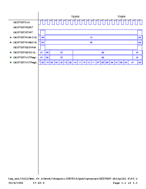
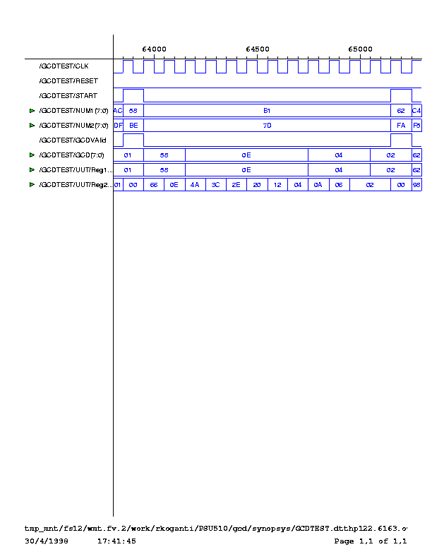
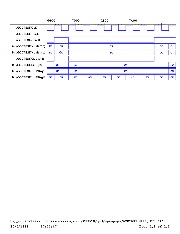
Some timing diagrams are presented here.
In the figure below the input number are (89)16 and (A4)16. 89 is placed on the NUM1 bus, A4 is placed on the NUM2 bus and the start signal is asserted. The GCDValid signal is asserted 20 cycles later, and the value on the GCDValid Bus is found to be 1.

For a Printable figure click here
In the timing diagram shown below, the input numbers are 58 and BE. The GCD is computed 13 cycles later and the value is found to be 02. The Reg1 and Reg2 values shown the intermediate values in the registers.

For a Printable figure click here
In the figure below, the input numbers are E0 and C0. The GCDValid signal is asserted 6 cycles later, and the GCD bus has the value (20)16.

For a Printable figure click here