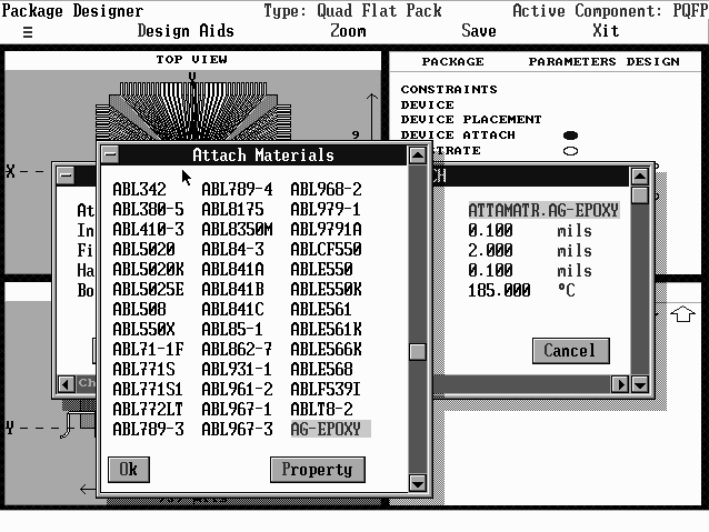
- Select the Parameters button to the right of the Device Attach command in the upper right quadrant. An Editing Die Attach window appears (see Figure 37). Its fields are defined below.
- Edit the fields you wish. Select the Accept button to accept the new data. Cancel to cancel. You will be returned to the Package screen.
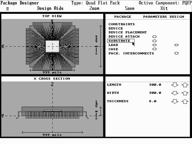
- Select the Parameters button to the right of the Substrate command in the upper right quadrant. An Editing Substrate window appears (see Figure 39). Its fields are defined on the next page.
- Edit the fields if you wish. Select the Accept button to accept the new data, Cancel to cancel. You return to the Package screen.
Definitions for Editing Device Attach Window
Some of the terms below are further defined in the Glossary in Appendix B.
Attach material: The material used to attach the device to the die. Material can be chosen from any library that exists in the material database. You can view the material properties of the attach material by selecting the Properties button, calling a Material Properties window. The fields in the Material Properties window are defined in the Glossary.
Initial horizontal crack depth: The maximum depth of the crack in mils, that exists along the x-axis of the chip, allowed by the screening process (internal visual inspection). This is an entry field. The range for this field is 0 to 5 mils.
Final horizontal crack depth: The crack depth, in mils, at which the crack along the x-axis of the chip causes failure. This is an entry field. The range for this field is 0 to 5 mils.
Half horizontal crack length: The length of the crack, in mils, that exists along the x-axis of the chip, allowed by the screening process (internal visual inspection). This is an entry field. The range for this field is 0 to 5 mils.
Bonding temperature: The temperature at which the active and passive devices (including die, capacitors and resistors) are bonded to the substrate or the package via the attach material. This is an entry field. Its range is 120 to 180 ° C.
Remember, you can use the Design Aids option, Section 6.3.1.2, to help you select a substrate technology.
Select the Substrate command from the upper right quadrant. The lower right quadrant window will be activated (see Figure 38). You can now vary the length, width, and thickness of the substrate, as explained on the previous page for the Device Attach command.
Editing the Substrate parameters
Some of the terms below are defined further in the Glossary in Appendix B.
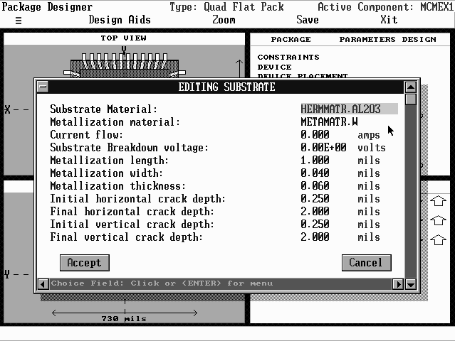
Substrate Material: The material the substrate is made of. This is a picklist field. You can view the material properties of the substrate material by selecting the Properties button. The fields in the Material Properties window are defined in the Glossary.
Metallization matr.: The material deposited on the surface of the substrate during metallization. This is a picklist field. You can view the material properties of the substrate material by selecting the Properties button. The fields in the Material Properties window are defined in the Glossary.
Metallization length: The length of the conductivity film deposited on the substrate during metallization. This is an entry field. The range for this field is 0-1000 mils.
Metallization width: The width of the conductive film deposited on the substrate during metallization. This is an entry field. The range for this field is 0-20 mils.
Metallization thickness: The thickness of the conductive film deposited on the substrate during metallization. This is an entry field. The range for this field is 0-10 mils.
Initial horizontal crack depth: The maximum crack depth, in mils, that exists along the x-axis of the substrate, allowed by the screening process (internal visual inspection). This is an entry field. The range for this field is 0-5 mils.
Final horizontal crack depth: The crack depth, in mils, at which the crack along the x-axis of the substrate causes failure. This is an entry field. The range for this field is 0-8 mils.
Initial vert. crack depth: The maximum crack depth, in mils, that exists along the y-axis of the substrate, allowed by the screening process (internal visual inspection). This is an entry field. The range for this field is 0-10 mils.
Final vert. crack depth: The crack depth, in mils, at which the crack along the y-axis of the substrate causes failure. This is an entry field. The range for this field is 0-10 mils.
Horizontal elliptic crack length: Surface length of an elliptic crack in the horizontal direction of the substrate, allowed by the screening process (internal visual inspection). This is an entry field. The range for this field is 0-10 mils.
Horizontal elliptic crack length: Depth of the elliptic crack in the horizontal direction of the substrate. This is an entry field. The range for this field is 0-10 mils.
Vert. elliptic crack length: Surface length of an elliptic crack in the vertical direction of the substrate, allowed by the screening process (internal visual inspection). This is an entry field. The range for this field is 0-100 mils.
Vert. elliptic crack depth: Depth of the elliptic crack in the vertical direction of the substrate. This is an entry field. The range for this field is 0-100 mils.
Bond pad pitch: The distance, in mils, between the centerlines of adjacent bond pads. This is an entry field. The range for this field is 0-100 mils.
Bond pad length: The length, in mils, of the area connecting the substrate to the package. This is an entry field. The range for this field is 0-80 mils.
Bond pad thickness: The thickness, in mils, of the area connecting the substrate to the package. This is an entry field. The range for this field is 0-100 mils.
Bond pad width: The width, in mils, of the area connecting the substrate to the package. This is an entry field. The range for this field is 0-100 mils.