- Select the Parameters button to the right of the Substrate Attach command in the upper right quadrant. An Editing Substrate Attach window appears (see Figure 40). Its fields are defined below.
- Edit the fields if you wish. Select the Accept button to accept the new data, Cancel to cancel. You return to the Package screen.
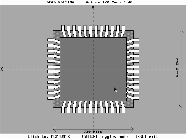
- Select the Lead command from the upper right quadrant. You will immediately be zoomed in on the top of the package, as seen in Figure 41.
- You may now select pins to edit. Pressing the Space Bar will toggle the mode between activate and deactivate. If the lead is white then it is activate, if it is cyan, the color of the case, then it is inactivate. In order to select pins you may either click on them individually with the left mouse button, or you may select a group by placing a box around them. This is done by clicking the left mouse button once in an area not inhabited by a lead. This will be one corner of the box, which is colored red. Move the mouse pointer to the opposite corner of the box such that the box completely encompasses those leads which you would like to edit. Press the left mouse button again to select the box.
- Press Esc or the right mouse button to return to the Package Design screen.
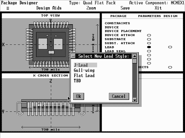
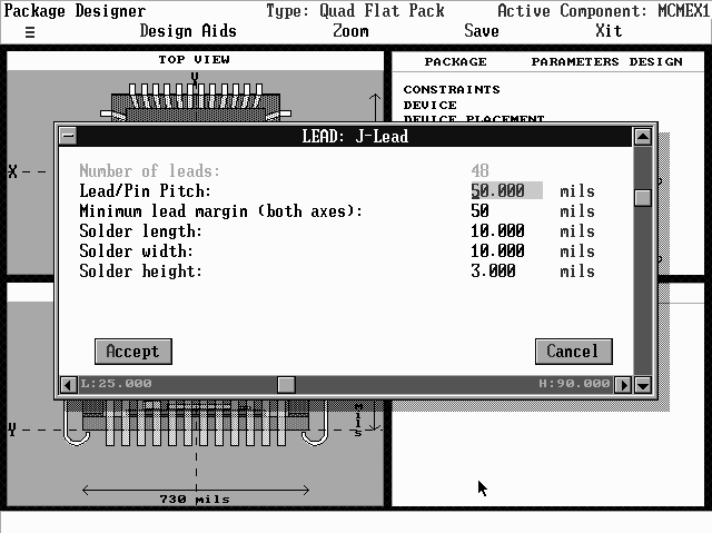
- Select the Parameters button to the right of the Lead command in the upper right quadrant. A window appears asking if you want to change the lead style. If you want to, or if you have yet to select one, select Yes. To skip this step select No. If you select Yes the window in Figure 42 will appear. You may now select the lead style which you wish to use. Note that the picklist selections are dependent on the type of package you are designing. A lead parameters window appears (see Figure 43). Its fields are defined below.
- Edit the field you wish. Select the Accept button to accept the new data, Cancel to cancel. You return to the Package screen.
- 6.3.4.6 The Subst. Attach Command
Select the Subst. Attach command from the upper right quadrant to edit substrate attach information. The lower right quadrant window will be activated. You can now vary the thickness of the substrate attach material using the same techniques you learned in Section 6.3.4.5.
Editing the Subst. Attach parameters
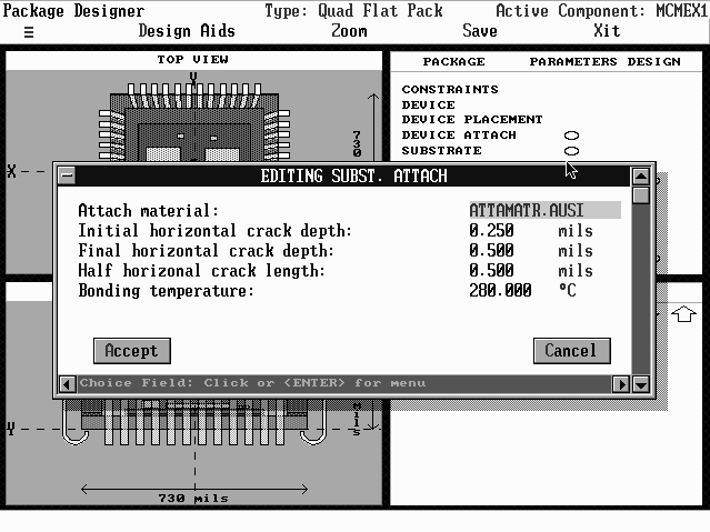
Definitions for Substrate Attach Window
Attach material: The material used to attach the device to the die. This is a picklist field. You can view the material properties of the attach material by selecting the Properties button, calling a Material Properties window. The fields in the Material Properties window are defined in the Glossary.
Initial horizontal crack depth: The depth of the crack, in mils, that exists along the x-axis of the substrate, allowed by the screening process (internal visual inspection). This is an entry field. The range for this field is 0-5 mils.
Final horizontal crack depth: The crack depth, in mils, at which the crack along the x-axis of the substrate cause failure. This is an entry field. The range for this field is 0-5 mils.
Half horizontal crack depth: The length of the crack, in mils, that exists along the x-axis of the substrate, allowed by the screening process (internal visual inspection). This is an entry field. The range for this field is 0-5 mils.
Bonding temperature: The temperature at which the substrate is bonded to the package via the attach material. This is an entry field.
The Lead parameter command does not enable you to edit lead dimensions. To do this, use the Lead command Design button, described in Section 6.3.4.7.1.
Pin Editing
The following instructions describe the pin editing process the activation
or deactivation of leads. Note that this function is only available for
PGA, Multi-inline, or similar packages.
Definitions for Lead Window
Number of Leads: The total number of leads on the Package, not including those which have been deactivated.
Notice that this field is grayed out, meaning it cannot be changed directly. The number of leads on a side is calculated by:
where, for both the x and y dimension, Nleads is the number of leads along that side of the package, Lpack is the length along that side, mpin is the pin margin for that side, and P is the lead pitch. The last two variables are located in this menu, while the length is controlled by the Case dimensions (see Section 6.3.4.11). For packages with pins, multiplying (Nleads)x by (Nleads)y and subtracting the number of deactivated leads gives the total number of leads.
Lead pitch: The distance, in mils, between the centerlines of the leads. This is an entry field. The range for this field is 1-500 mils.
Minimum lead margin (x-axis): The minimum distance from the edge of the package to the first lead on the x-axis side. This is an entry field. The range for this field is 1-500 mils.
Minimum lead margin (y-axis): The minimum distance from the edge of the package to the first lead on the y-axis side. This is an entry field. The range for this field is 1-500 mils.
Lead protrusion: The length of that section of the lead that penetrates beyond the package wall. This is an entry field. The range for this field is 7-500 mils.
Solder length: The length of the solder pad connecting the lead to the next packaging level. This is an entry level. The range for this field is 1-40 mils.
Solder width: The width of the solder pad connecting the lead to the next packaging level. This is an entry level. The range for this field is 1-40 mils.
Solder height: The height of the solder pad connecting the lead to the next packaging level. This is an entry level. The range for this field is 1-3 mils.
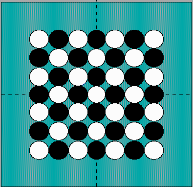
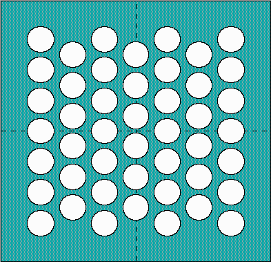
I/O Configuration: The layout of the pins. This field is not applicable in packages without pins. Not Staggered is an even distribution across the surface area. Staggered has the even columns offset down by ½ pitch, with the last even column removed. Checkerboard has alternating pins removed from the Not Staggered layout. See diagrams below.