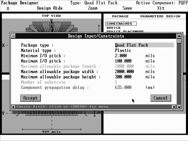
- Select the Constraints command in the upper right quadrant. The window in Figure 26 appears. The window contains numerous categories of constraints. You must assign data to each category field. The fields are defined on the next page.
- Select field in turn and assign data. An acceptable range of values appears at the bottom of the screen for each numeric field. If you assign a value outside the range, the minimum or maximum value is automatically assigned a package length or width that is larger than the substrate length or width.
- Select the Accept hot key to accept changes, Cancel to cancel. A window asks you to confirm changes. Pressing Esc also displays such a window. You return to the Package screen.
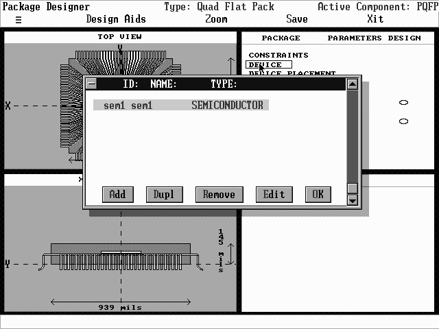
- Add enables you to add and place devices.
- Duplicate allows you to create duplicate devices.
- Remove enables you to remove devices.
- Edit enables you to edit existing devices.
- OK will save and exit the menu.
- Select the Add button from the Device window. A Specify Type window appears.
- Select a device typeCapacitor, Resistor, Semiconductor, or focal plane array. The window in Figure 30 appears. If you select Semiconductor, a window first asks for its orientation. Select a flat or edge orientation. Flat orientation means the die is mounted flat on the substrate or case. Edge orientation means the die is mounted on one of its edges, i.e., face formed by the length, width, and thickness dimensions.
- Fill in the element ID and name fields. The other fields vary, depending on the type of element selected. The fields are defined on the next page.
- When finished assigning values, select the Accept button to accept, Cancel to cancel and return to the Package screen.
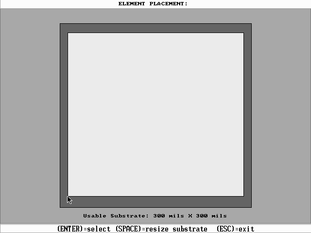
- Accepting the values returns you to the Package graphical interface. The new device appears in the package (see Figure 31). Hold down the left mouse button and move the pointer or use the arrow keys to position the device. Press R to rotate the die 90 degrees. Press Esc to cancel at this point.
- Press the left mouse button or Enter when the device is positioned correctly. The device cannot overlap or be on top of another device or an error message appears. After placing, you return to the Device window. You can add more devices or exit to the Package screen.
- If the device is larger than the substrate, you can increase the size of the substrate before placing the device. Press the Space bar. A substrate Size message appears. Press the left and right arrow keys to increase the length, the up and down arrow keys to increase the width. You will be constrained by the base length and width and the size of any dies already placed. Press Esc when you finish resizing the substrate. You can now place the device.
- 6.3.4.1 The Constraints
Command
In all parameter editing windows in the package designer, fields that are colored BLUE indicate that field has not been edited yet by the user; BLACK fields have been edited; and GREEN fields are currently unused by any modules in CADMP-II.
Before you can use any of the other commands in the upper right quadrant, you must specify the design constraints. Examples of constraints include the number of I/O the package must accommodate and minimum I/O pitch. If a category is grayed out you cannot change it. However, values entered in other fields may change the grayed-out value. The purpose of the screen is to constrain package design options to those which allow the part footprint to fit into the overall assembly design.
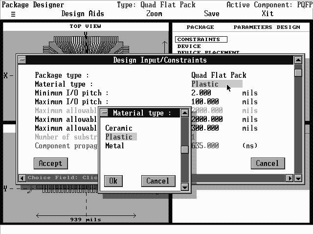
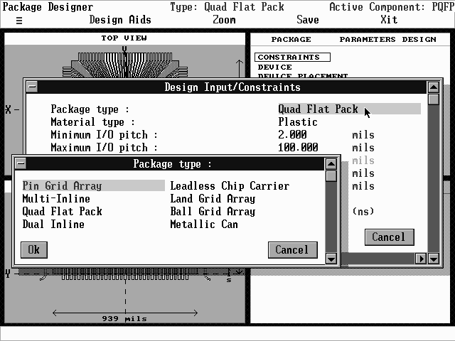
Selecting some categories displays a pick list window (see Figures 27 and 28). See the definitions on the next two pages for details.
Definitions of Terms Found in the Constraints Menu
Some of the terms below are further defined in the Glossary in Appendix B. The acronym "TBD" means "To Be Determined."
Package type: The type of package specified. This is a pick list field. Your choices are constrained by the mounting technology you choose.
Material type: The package material is specified in this field. This is a pick list field.
Min/Max I/O pitch: the distance, in mils, between the centerpoints of adjacent inputs and outputs. This is an entry field. The range for this field is 0 to 200 mils.
Maximum allowable package length: The maximum length, in mils, of the package. This is an entry field. The range for this field is 100 to 5000 mils. The maximum package length you enter is an upper bound on the length value and is treated as a space constraint.
Maximum allowable package width: The maximum width, in mils, of the package. The width is determined by the length.
Maximum allowable package height: The maximum height, in mils, of the package. This is an entry field. The range for this field is 1 to 1000 mils.
Number of substrate: Number of substrate layers in the package. This is an entry field. The entry for this field must be either 0 or 1.
Component propagation delay: The delay between the component input and component output of a signal. Typically, the delay time is measured in nanoseconds. This is an entry field. The range for this field is 1 to 1000 nanoseconds.
Max. die processing temperature: This is the maximum temperature the die can withstand during processing of the die for the package. This is an entry field. The range for this field is -55 to 500 ºC.
Outer-interconnect technology: The interconnect technology used to connect the substrate to the leads. This is a pick list field.
Minimum metal trace pitch: This is the minimum distance between two metallization lines. This is an entry field. The range for this field is 1 to 9.8 mils.
Maximum allowable package weight: The maximum weight, in kilograms or grams, of the package. This is an entry field. The range for this field is 10 to 1000 g.
Maximum allowable lid deflection: The maximum allowable deflection (bending or distortion), in millimeters or mils, of the package lid. Maximum allowable lid deflection means the distance to contact any package device, including 3-D die stack. This is an entry field. The range for this field is 0 to 15 mils.
Package standoff from mounting platform: The height, in millimeters or mils, of the metal post connecting the package to the mounting platform. This is an entry field. The range for this field is 0 to 39.37 mils.
Lead attachment to case: The method used to attach the lead to the case. This is a pick list field.
Allowable junction temperature: The maximum temperature, in degrees Celsius or Fahrenheit, at the semiconductor junction (i.e. hot spot on the chip). This is the worst case safe operating junction temperature. This is an entry field. The range for this field is -55 to 200 ºC.
Max. allowable lead resistance: The maximum resistance, in ohms per inch or ohms per centimeter, the lead offers. This is an entry field. The range for this field is 1 to 3 ohms/in or .394 to 1.181 ohms/cm.
Max. inductance of interconnects: The maximum allowable interconnect inductance, in Henrys. Typical values of maximum inductance for various interconnects is given in Design Aids in the Lead Inductance category. This is an entry field. The range for this field is .05 to 5 nH.
Max. signal noise: The maximum amount of unwanted electrical signal produced during normal interconnect operations. Measered as a percentage of voltage input. This is an entry field. The range for this field is 1 to 100% of voltage input.
Maximum unit cost: The maximum cost of the package, in dollars. This is an entry field.
Production volume: The number of packages to be produced. When you select this field, a window appears asking you to choose between "Entry Value" and "TBD" (To Be Determined). If you select Entry Value, another window appears asking you to input the package production volume.
Mounting platform material: The material used to mount the components on the substrate. This is a pick list field.
Expected mounting platform temperature: The temperature, in degree
Celsius or Fahrenheit, experienced by the mounting platform. This is an
entry field. The range for this field is 30 to 80 ºC.
Use the Device command to specify the active and passive devices that form the package circuitry.
Select the Device command in the upper right quadrant. The window in Figure 29 appears. The window has five buttons:
Definitions of Terms found in the Elements Menu
Some of the terms below are further defined in the Glossary in Appendix B. Note that when you select Device, you can choose among three types of elements: capacitor, semiconductor, and resistor. Each choice calls a different parameter window. Each window is defined below.
If you select Capacitor
Element ID: An alphanumeric identification you assign the element.
Element name: The name you give the capacitor. This is an entry field.
Element technology: The technology used to produce the element. This is an pick list field.
Capacitance: The capacitance (amount of charge that can be stored per unit potential difference between conductors), in farads, of the capacitor. This is an entry field. The range for this field is 0 to 1.00E+02 farads.
Capacitor tolerance: This tolerance is stated as the maximum positive and negative deviations of capacitance from rated nominal values at a standard test temperature (typically 25 ±3ºC), measured at a standard frequency (typically 1 volt). It is usually expressed as a percentage of the nominal capacitance.
Element length: The length, in mils, of the element along the x-axis. This is an entry field. The range for this field is 1 to 1000 mils.
Element width: The width, in mils, of the element along the y-axis. This is an entry field. The range for this field is 1 to 1000 mils.
Element thickness: The length, in mils, of the element along the z-axis. This is an entry field. The range for this field is 1 to 1000 mils.
Allowable operating temp: Capacitance of a capacitor typically varies with temperature. The field specifies the maximum value of opeating temperature for the capacitor.
Working voltage: This is the maximum voltage at which a capacitor may be operated continuously over its rated operating temperature range. This is an entry field. The range for this field is 0 to 5 KVDC. K means x1E3.
ARC voltage: The arc voltage or the surge voltage is the maximum DC voltage, including peak AC or other pulses, which may be applied for a short duration. This is an entry field. The range for this field is 0 to 10 KVDC.
Dissipation factor: Dissipation factor is the ratio of the effective series resistance of the capacitor to its reactance at specified frequency. (Also see the Glossary). This is an entry field.
Comments: A field in which you can enter notes.
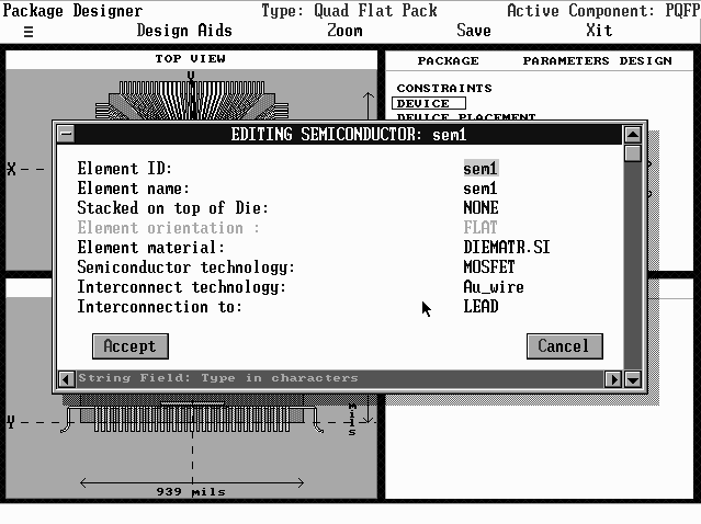
If you select Semiconductor
The Semiconductor parameter window contains six fields that are defined
exactly as in the Capacitor selection, with exactly the same ranges for
their values. They are: Element ID, Element name, Element length, Element
width, Element thickness, and Comments. The other fields in the Semiconductor
parameter window are defined below:
Element orientation: Whether this type of semiconductor is placed flat or on its edge. You cannot modify this field.
Semiconductor technology: The type of semiconductor used. This is a pick list field.
Element material: The material the semiconductor is made of. This is a pick list field. Press the Space bar to display a list of materials.
Interconnect technology: The type of interconnect used. This field consists of two pick list windows. When you first select the Interconnect technology field, a Select Tech. window appears. After you select a technology from the list in this window, a second Select Tech. window appears. You can view the parameters of the technologies in the second window by selecting the Parameters button. A parameters window appears. The window fields are defined in the Glossary.
Power dissipation: The heat generated by the device, in watts. This is an entry field. The range for this field is .00001 to 1000 watts.