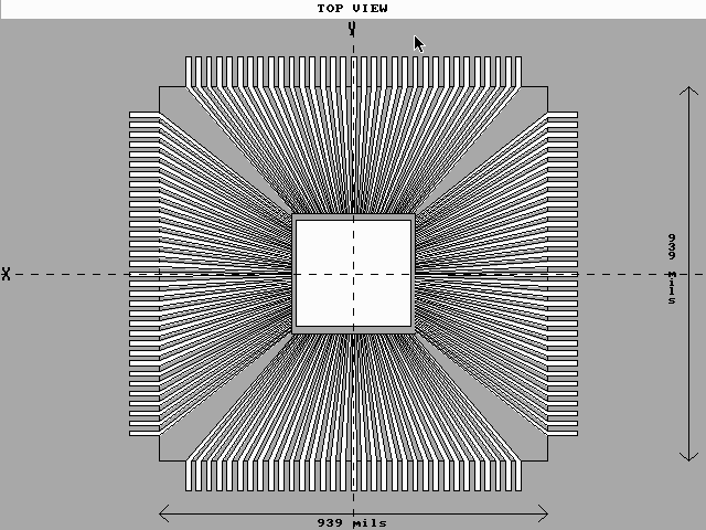
- The Top command enables you to view an enlarged top view.
- The X-cross command enables you to view an enlarged x-cross section view.
- The Y-cross command enables you to view an enlarged y-cross section view.
- Select the Top command from the Zoom menu. A window like the one in Figure 24 appears.
- Press Esc to return to the Package screen.
- Definitions of Terms found in the Design Aids
Interconnects
Min. chip I/O pitch: The minimum chip I/O pitch, in mils, refers to the currently attainable center-to-center spacing between the die bond pads.
Max. I/O count: The maximum I/O count is the current maximum number of interconnect terminals that a technology can interconnect. Often, high I/O counts and low pitches are limited by interconnection manufacturing process constraints.
Lead inductance: The amount, in nanoHenrys, of the lead property that opposes a change in current flow which causes current changes to lag behind voltage changes. High-frequency applications require careful control of the lead inductance. The inductance of an interconnection is dependent on the dielectric constants of the connected materials, the geometry of the signal path, and the existence and location of the reference plane(s).
Mutual inductance: The amount, in nanoHenrys, of the interconnect property that opposes a change in current flow which causes current changes to lag behind voltage changes. High-frequency applications require careful control of the mutual inductance between the interconnects.
Area array potential: The ability of inner-interconnect to connect the chip or the substrate to the leads when the leads are arranged in a matrix format on the package base like the PGA.
Packaging efficiency: Packaging efficiency is the ratio of the total area of the active elements (dies) to that of the pad pitch footprint of the package. The packaging efficiency depends on the connection technique, package type, package outline, and pad pitch.
Testability: Manufacturing yield considerations often demand that the die be tested before being packaged to reduce rework costs, Pre-testability is usually achieved by using surface probes on the die, and is limited by pitch and die sizes. Testability is important because if a die is found to be defective after being mounted on a substrate, replacing it results in added cost and, sometimes reduced quality.
Loop control: Loop control is the ability to produce a particular profile in an interconnect wire loop. While high loops help the bond to survive temperature cycling, a high loop increases the height of the package and the interconnection length. In plastic packages, if the wire loop is too high, the molding process may cause wire sweep and subsequent wire breakage or disconnection from the pad.
Flexibility: Flexibility indicates the capability of an interconnection technique to adapt to a design or process parameter change.
Die availability: Die availability indicates the ease of obtaining suitably prepared dies for an interconnection technology. TAB, flip-TAB, and flip-chip may require die bumping, a complex process step not available for all devices. Wirebonds and most high-density interconnects do not require any special processing of the pad bumps.
Tool availability: Tool availability reflects the maturity and cost of equipment for an interconnection technique.
Dominant failure mechanisms: The mechanism by which mechanical, thermal, electrical, radiation, and chemical stresses cause wearout or overstress failures of package elements.
Process complexity: Process complexity states qualitatively the effort required to design the interconnect. While for mature interconnect technologies such as wire bonding often a software change is required for design iterations, a design change in TAB or flip-chip is a hardware change. Further, the design variables and their interactions are far more complex for technologies such as HDI.
Technological maturity: Technological maturity describes the relative developmental status of an interconnection technique and provides a measure of the risk of using it, based on years of use and frequency of changes made to the manufacturing processes.
Heat dissipation: Heat dissipation quantifies the capability of an interconnection technology to remove heat from the active elements during device operation.
Ability to rework: Rework depends on the availability of special tools and techniques to debond active and passive elements while maintaining the integrity of the substrate and metallization.
Market share: Market share refers to the portion of the market claimed by a specific interconnection technology.
Cost: Cost refers to the overall expense of implementing an interconnection technology, and is dependent primarily on manufacturing requirements and the feasible degree of automation.
Substrate Technology
Dielectric constant: That property of a dielectric which determines the electrostatic energy stored per unit volume for unit potential gradient.
Max. signal layers: The maximum number of signal layers allowed for routability purposes.
Min. metal. pitch: The minimum center to center distance, in micrometers, between the metallized strips placed on the substrate during metallization.
Thermal conductivity: The ability of a material to conduct heat; the physical constant for the quantity of heat that passes through a unit cube of a material in a unit of time when the differences in temperature of the two faces is one degree Celsius.
Maximum area: The maximum area, in square centimeters, the substrate can occupy.
Substrate I/O style: The substrate I/O style will either be area array, in which package leads are arranged in an array, as in a PGA, or peripheral, in which package leads are arranged along the boundary of the substrate or chip.
Package Type and Mounting Technology Categories
Currently attainable I/O pitch: Same as minimum I/O pitch
in interconnect definition.
Typical Maximum I/O count: Same as Maximum I/O count in interconnect
definition.
Packaging Efficiency: Same as interconnect definition.
Performance: Refers to a lead or package styles capability in terms of check frequency, propagation delay, and signal noise.
Package Cost: Same as interconnect definition.
Heat Removal: The ability of a mounting technology or package type to conduct heat from the chip to the package outside.
Package Profile: The package height typical of a package type.
Testability: Same as interconnect definition.
Visual Inspection: The potential of using visual inspection for quality assurance/inspection. Though visual inspection is possible in dual-in-line packages, it is hardly feasible in land-grid arrays, where more advanced techniques like acoustic microscopy and x-ray imaging need to be used.
Rework: Same as interconnect "ability to rework" definition.
6.3.2 The Zoom
Option
The Zoom option contains three commands:

The X- and Y-cross commands work the same way
The Save option saves changes to the package design.
6.3.4 The Package Screen Parameters Quadrant
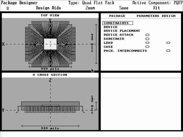
The upper right quadrant of the Package screen (see Figure 25) functions like an option header and enables you to specify package parameters. Commands are listed at the far left of the quadrant under the heading "Package." These commands function like commands in the option header menus. Some have an oval button immediately to the right under the category "Parameters." Click on these buttons to display windows enabling you to view and edit parameter data. The Lead and Interconnects commands have buttons at the far right of the upper right quadrant under the category "Design." Click on these buttons to display windows enabling you to view and edit design data.

Note: You CANNOT exit these Design button windows by pressing the right mouse button. To exit these windows without saving changes, press Esc or move the pointer to the small button in the upper left corner of the window and press the left mouse button.