- identification of potential failure sites; failure mechanisms (chemical, electrical, mechanical, and thermal processes leading to failure); and failure modes (observed forms of failure such as shorts, opens, or electrical deviations beyond specification).
- identification of the appropriate failure models and their input parameters, including those associated with material characteristics, damage properties, relevant geometry at failure sites, manufacturing flaws and defects, and environmental/operating loads.
- computation of time to failure for potential failure mechanisms.
- accepting the design, if the estimated minimum time to failure is greater than the desired design life.
- performing a sensitivity analysis which reveals the sensitivity of the package lifetime to the package geometry, material properties, operating conditions, and environmental attributes.
- altering design parameters, according to sensitivity analysis results, to raise the minimum time to failure to the desired design life.
- designing packages for user-specified functional requirements;
- assessing component reliability during the design phase;
- evaluating new materials, structures, and technologies;
- assessing packages designed by other software programs or manufacturers
- guiding the development of accelerated tests and screens
- It cannot be used to design semiconductor chips on active/passive devices. Functional device parameters are assumed to be given at the start of the design process.
- It cannot be used to analyze problems due to mishandling and poor application.
- It does not address software reliability.
- CADMP-II is not a functional circuit design tool.
- All package elements are not implemented. Future package elements and architectures will be incorporated as per the requests of CADMP-II members.
- Manufacturing considerations are not yet incorporated.
- The failure algorithms do not yet incorporate models with integration, differentiation, summation, sec, cosec, cotan, or iterative algorithms.
- All failure mechanism models must be in terms of package attributes recognized by CADMP-II.
- Reliability estimates do not specify probablistic variations in geometries, materials and defects. However, sensitivity analysis is possible and allows the design team to do single variable analysis to evaluate the impact of parameter variabilities for any of the failure mechanisms versus their choice of environment, test/stress, package, or material parameters,
- Material property dependencies are limited to temperature, frequency, moisture and strain rate. Multiple dependencies cannot be handled. Only temperature dependencies are currently used by CADMP-II.
- Some of the materials in the Materials Library lack some of the properties necessary for analysis. This is because many material electronic properties are either unknown or poorly documented and may not be used to optimize design or predict reliability. The distribution of material property data is key to reliable electronic component design and accurate reliability modeling. Variability data is lacking for most component and sub-assembly properties. In addition, test methods are not standardized, resulting in poorly documented physical property values. CALCE EPRC has written several proposals to address this problem and is in the process of establishing a national resource center for material characterization and a comprehensive database.
1.1 The Physics of Failure Approach
Computer Aided Design of Microelectronic Packages (CADMP-II) is a set of integrated software programs that assist in the design and analysis of a microelectronic package. The software uses the physics of failure approach based on a scientific determination of the dominant failure mechanisms and failure sites within the component. The dominant mechanisms are determined by using accepted models to calculate the time to failure for each of a series of potential failure mechanisms and identifying which cause failure within the desired mission life. The dependence of the time to failure on the package attributes and the environmental/operational stresses is also determined for each dominant mechanism.
The results of this physics of failure analysis allow a designer to choose package geometries and materials which reduce the risk of failure by the identified mechanisms. This makes reliability assessment a part of the design process rather than just a tool for predicting the useful life of an existing product. In addition, the analysis can be used to plan tests and screens, and to determine electrical, mechanical, and environmental stress margins.
The following steps are involved in a physics of failure analysis:
1.2 An Introduction to the CADMP-II Electronic Package Design Process
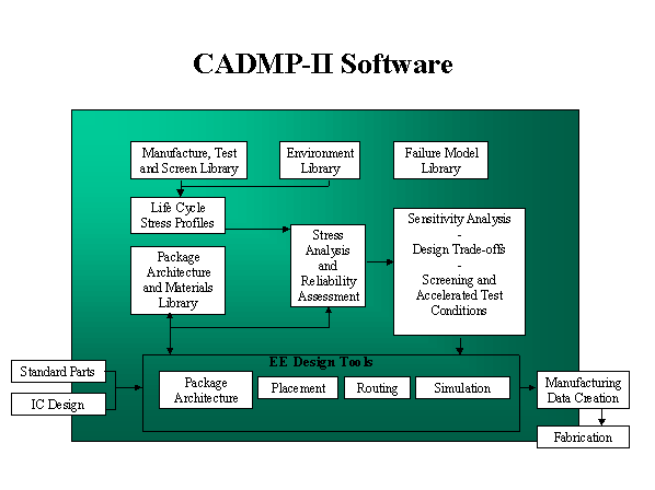
The flow-chart shown in Figure 1 shows where CADMP-II fits into the microelectronic design process as a whole. The purpose of CADMP-II is to assess the thermal, electrical, and mechanical performance of a package and to indicate the design trade-offs, qualification, and quality assurance procedures needed to produce the package. This knowledge is used with electrical engineering software, where final geometries, component placement, and circuit routing are developed.
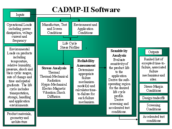
In order to use CADMP-II to its
fullest, the user must understand what the required inputs are. These are
shown in Figure 2. Note that as a physics-of-failure tool, CADMP-II requires
the user to specify the operational and environmental loads that the device
must endure over its mission life. In addition, complete data on the package
and die material properties, geometry, and architecture is required to
perform a complete reliability assessment. If an attribute is neglected,
the failure models which require that information cannot be evaluated.
Operational and environmental load data combined with test/screen conditions are used to create the mission profile of the device. Geometrical information is input into a package designer interface. Materials from the materials library are assigned to each package element. The package designer contains easy to use guidelines to quickly and efficiently walk the user through the modeling process.
All of the above information is used to conduct four basic analyses: thermal, reliability, sensitivity, and accelerated testing.
The thermal analysis uses a three dimensional finite-difference approach to calculate the temperature distribution within the package. The analysis can be performed using either conduction or convection with conduction.
Reliability assessment allows the user to select relevant failure mechanisms and determine the average time-to-failure of all package elements for the specified mission profile and package design using physics-of-failure models stored in the failure mechanism library. Figure 3 outlines the classification of failure models in CADMP-II.
After the reliability assessment has been performed, a sensitivity analysis can be performed. For a wearout failure model, the analysis identifies the sensitivity of the average time to failure of the package to variations in critical parameters. Overstress models allow the same calculation for the stress margin. Graphical results for the sensitivity analysis can be either in the form of a comparison of one parameter versus the time-to-failure (TTF), or as one parameter versus another with iso-TTF curves.
CADMP-II also contains an accelerated testing tool. Through the use of this tool, the user can determine testing levels based on failure mechanisms, failure modes, and stresses for the particular application. Accelerated testing parameters are based on the knowledge of the dominant failure mechanisms obtained from the reliability assessment tool. In this way, the stress levels incorporate the geometry, materials, and manufacturing processes of the package.

1.3 Limitations of the Software
1.4 Manual Outline
In the following chapters, the CADMP-II system architecture will be discussed. Chapter 2 explains the hardware and software requirements and provides CALCE EPRC software support information. Chapter 3 explains installation and introduces the user to the CADMP-II system. Chapter 4 introduces the tools available in the software: parts, modeling, analysis (thermal, reliability, sensitivity, and accelerated testing), and the libraries. Chapters 5 through 8 provide descriptions of the purpose, and detailed instructions, for each of these tools. Appendices are provided at the end of the manual. Appendix A is a set of tables and validation histories for the constants and exponents used in the software. Appendix B is a glossary of material properties, and Appendix C provides variable definitions and dimensional diagrams.