- Select the Parameters button directly to the right of the Mounting Platform command. An Editing Mounting Platform" window appears. The fields are defined below.
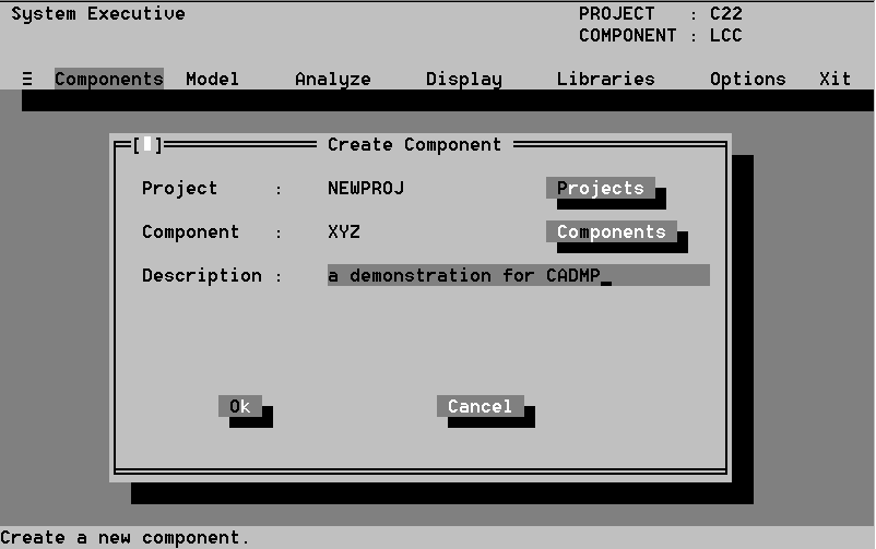
- To design a new package, select the New option under the Components menu in the System Executive. A Create Part Data window appears (see Figure 62).
- Specify a Project name, an ID, and a description of the component in the corresponding fields. The window will display the name of the user creating the part.
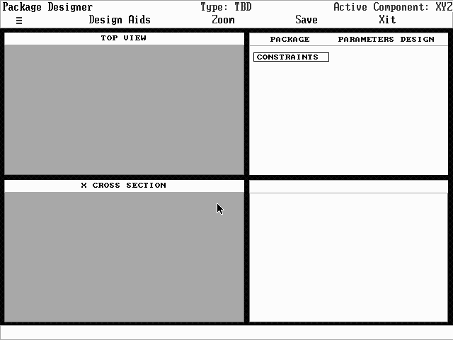
- Select OK to accept the part, Cancel to quit without saving. Exit the Create Componenet menu, and enter the Model menu and then pick Package. The Package graphical interface in Figure 63 appears if you accept the part.
- Specify the constraints for the new package in the same way you edited constraints for the pre-existing designs (see Section 6.3.4.1). Remember, you must define constraints before attempting to select the other options in the Package window. Otherwise, a message appears reminding you to define the constraints.
- Specify package elements the same way you edited element for ore-defined package in Section 6.3.4.2.
- Save the new package design by selecting Save.
- Select Xit to exit the package designer.
- If you select Xit without first saving your package, the screen will ask you if you would like to save the changes.
- Select Yes to save, No to return to the previous design and exit.
- If you select Yes, the screen will display a message indicating it successfully saved the package. Select OK to clear the screen.
- Now select Xit to exit the package designer.
- Definitions for the Interconnects Command
Substrate interconnect: The technology selected to make the interconnect from the substrate to the package. This is a picklist field, consisting of three windows. The first window that appears when you select the field, "Select. Tech," enables you to select a technology to use for the interconnect. After you select the technology, a second "Select Tech." Window appears, offering you subcategories from which to choose. You can view the parameters of these subcategories by selecting the Parameters button, calling a Parameters window. The fields in the window are defined on this page. If an acceptable interconnect is not present, create one in the Interconnect Library (see Section 6.4.2) and then select it with the Interconnect command.
Die Interconnect: The technology selected to make the interconnect from the die to the substrate.
Wirebond Technology Window
Wire material: The material the wire is made of.
Bond type: The method used to bond the interconnect to the package.
Length of the wire bond: Length of the wire actually bonded to the bond pad surface.
Wire span: Straight-line distance between first and second bond of wirebond interconnect.
Wire diameter: The diameter of the wire used to bond the interconnect to the package.
Wire length: The total length of the wire in making a wire bond interconnection.
Init. Radius of curve: Radius of curvature of the wire at the first and second bonds.
Angle of wire with substrate: Angle that the wire makes with the bond pad in radians.
Resistance of wire per unit length: Resistance measured in ohms per unit length allocated to the first-level interconnect.
6.3.4.13
The Modeling Compounds Command
Select the Molding Compound command in the upper right quadrant. The lower right quadrant is activated. You can now vary the width, thickness, and inside width of the molding compound encapsulating a BGA package using the technique learned Section 6.3.4.4.
Editing the Molding compound Parameters
Select the Parameter button
directly to the right of the molding compound command. An Editing Molding
Compound window appears. Double click on the material to the right of the
title molding compound material" to change the selection. A Select Library
window appears. Choose "Plastic Package Materials" by highlighting it and
pressing OK. A Plastic Material Window Appears. You may view the
properties of several compounds before making a choice. Once you have selected
a compound, press OK followed by ACCEPT to return to the
package screen.
6.3.4.14 The Mounting Platform Command
Select the mounting platform command in the upper right quadrant. The lower right quadrant is activated. You can now vary the width and thickness of the platform on which the die is mounted in a PBGA using the techniques learned in Section 6.3.4.4.
Editing the Mounting Platform Parameter
Platform material: the printed wiring board type metal coated laminate material onto which the semiconductor device is mounted and through which signals are transmitted from the die to the solder ball interconnects.
Number of Layers: number of signal carrying metal layers in the mounting platform laminate.
Applied voltage: Standard operating voltage for the device.
Exiting the package designer