Microwave Circuit Design: Lab 5
© B. Pejcinovic, P. Wong, O. Woywode
Introduction
This lab investigates how trade-offs between gain and noise figure
affect the design of an amplifier.
Design Specifications

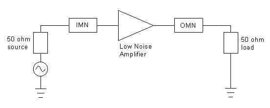
Figure 1: Block diagram of an amplifier
You are to design a single-stage amplifier that has a noise figure
(NF) of 1.8 dB and an available gain (GA)
of 20 dB. The design frequency is f = 1 GHz.
The core of the schematic is a special low noise amplifier (LNA)
subcircuit. MDS supplies a pre-built LNA subcircuit (called LS_amplifier)
as part of its demo files. You still have to add a few extra components
to the LS_amplifier subcircuit to
create the final LNA subcircuit.
There is a 50 ohm source impedance on the input side of the LNA
and a 50 ohm load on its output. To keep things simple, use ell
circuits (i.e., capacitors and inductors) instead of microstrip
for the input and output matching networks. You may also ignore
coupling capacitors.
Accessing the Pre-built LNA Subcircuit
If you already have both the samplelib
and Learn_amp icons on your main
MDS screen, then you may skip the following procedures. If you
do not have those icons visible, then perform the following
procedures to load the necessary MDS library files:
Loading samplelib:
Activate the file browser utility either by choosing [MB:TOOLS/BROWSE-OPEN]
or by clicking [SUI:Browse/Open]. The 'Browse/Open' dialog
window appears. At the top of the window, click [Unix System]
to view your Unix directories. Next click [Browsing Options…].
When the 'Browsing Options…' window appears, click [Libraries]
to view only MDS libraries and then click [OK] to exit.
In the center of the 'Browse/Open' window, you should now see
a scrollable list of available MDS libraries. Scroll down the
list, select the samplelib library,
and click [OK]. The 'samplelib: FILE' window will appear. Close
that window.
Loading Learn_amp:
Activate the file browser utility again. In the 'Browse/Open'
dialog window, click [Browsing Options…]. Click [Working]
to view your current working directory and then click [OK] to
exit.
In the center of the 'Browse/Open' window is an input box labeled
Directory path, which shows the name of your current directory.
Below that is a scrollable list of directories and files that
you can click on to navigate the directory system. Erase whatever
text is in the input box and type /pkgs
(i.e., a forward slash character followed by the directory name
pkgs) In the scrollable list area,
successively click on directory names in this order:
hp_hfds-7.0/ --> mds_b.07.00/
--> hp85150/ --> demos/
Once you are in the demos/ directory,
scroll down the list, select the Learn_amp
file, and click [OK]. The 'Learn_amp: FILE' window will appear.
Open the LS_amplifier icon and examine
the low noise amplifier schematic. When you are done, close the
open windows.
Creating the Final LNA Subcircuit
Assignment
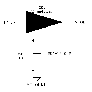
Create the LNA subcircuit that contains both the LS_amplifier
subcircuit and its DC power supply.
Circuit construction

Figure 2: LNA subcircuit (LS_amplifier
+ power supply)
- Construct the subcircuit shown in Figure 2. To access the
LS_amplifier subcircuit, click [MB:INSERT/COMPONENT/BY
LABEL]. The 'Label of Design Icon to be used as a Component:'
window appears. In the input box, type Learn_amp/LS_amplifier.
Click [OK] and then place the LS_amplifier
symbol onto the circuit page.
- Add the +12.0 volt DC power supply and the input and output
connectors to LS_amplifier. To finish
the LNA subcircuit, remember to create a symbol and add the reference
block (i.e., use [MB:WINDOW/CHANGE PAGE/SYMBOL 2], [MB:PERFORM/CREATE
SYMBOL], and [MB:INSERT/REF-NAME-LABEL]). When done, close the
LNA subcircuit window.
LNA Noise Characteristics
Assignment
You will determine the noise figure characteristics of the LNA
subcircuit.
Circuit construction

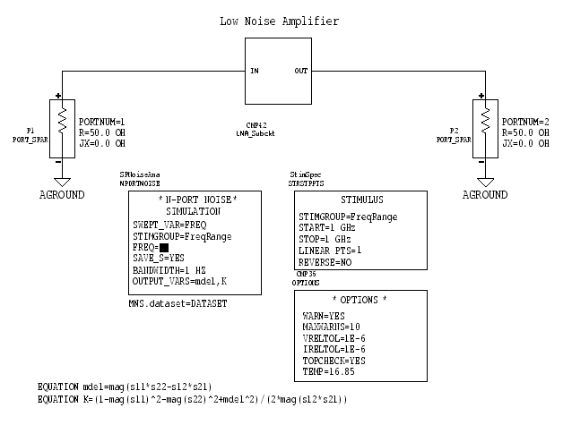
Figure 3: LNA test circuit
NOTE: The circuit in Figure 3 was created using a template
that has all the necessary noise and stimulus controls pre-configured.
Do not try to build the circuit using your standard construction
techniques. Perform the following steps instead.
- Create a new circuit page.
- Select [MB:INSERT/TEMPLATE/templatelib/S_Parameters/Noise_vs_freq].
An outline of an entire test circuit tags along with the mouse
pointer. Click the mouse button to drop the noise vs. freq test
circuit onto the circuit page.
- Delete the text on the circuit page that says [CONNECT
YOUR CIRCUIT HERE]. Insert your LNA subcircuit in the spot
where the deleted text used to be.
- Add the two equations to the circuit page.
- The line that says MNS.dataset=DATASET tells MDS to
use the name DATASET when saving
the data from the simulation run. It is not a simple line
of text. Choose [MB:INSERT/MNS/DATASET NAME]. Position the mouse
pointer where you want the MNS.dataset= line to appear
and click the mouse button to drop the line onto the circuit page.
You can change the dataset name to something else if you wish,
as long as you remember to use the same name on your presentation
pages.
Simulation
NOTE: Instead of using the standard 'Simulation Setup'
dialog window to configure the simulation, you will edit the parameters
of the noise and stimulus control boxes that reside on the circuit
page.
- In the control box labeled STIMULUS, make the following
changes:
START=1 GHz, STOP=1 GHz, LINEAR PTS=1
This sets the frequency sweep to a single point at 1 GHz.
- In the control box labeled N-PORT NOISE SIMULATION,
make this change: OUTPUT_VARS=mdel,K
This declares the equation variables mdel and K
as output variables.
- To actually run the simulation, first highlight the N-PORT
NOISE SIMULATION control box by clicking inside that box.
On the left side of the circuit page window is a column of command
buttons. Click the [S] button to start the simulation.
Output
- When the simulation is done, create a new presentation page.
Be sure the Dataset= line at the top of the presentation
page has the correct dataset name.
- Choose [MB:INSERT/TEMPLATE/templatelib/S_Parameters/Noise_vs_freq].
A very large outline of several output plots tags along with the
mouse pointer. Click the mouse button to drop the plots onto the
presentation page.
- Carefully examine each of the plots and note the significance
of the various parameter values.
Items to turn in
- Turn in printouts of the LNA subcircuit (see Figure 2) and
the LNA test circuit (see Figure 3).
- Submit a printout of the presentation page containing the
noise figure plots.
Questions
- According to the noise figure plots, what is the minimum noise
figure NFmin? (NFmin in the plot)
- What is the equivalent unnormalized noise resistance Rn?
(RN in the plot)
- What is the stability of the LNA subcircuit at 1 GHz? Explain
how the stability regions of the LNA subcircuit might affect your
choice of source and load reflection coefficients.
Matching Network Design
Assignment
The amplifier design requirements are NF = 1.8 dB and GA
= 20 dB at f = 1 GHz. Find the source and load reflection
coefficients that will accomplish this goal. Design the corresponding
input and output matching networks using ell circuits.
NOTE: This is a paper design only. You do not need to construct
and simulate the IMN and OMN.
Design considerations
One way to approach this design is to plot the 1.8 dB noise figure
circle and the 20 dB available gain circle on the same Smith chart.
The intersection points between the two circles will tell you
the required source reflection coefficient.
- Create a new presentation page. Instead of plotting a Smith
chart the standard way, choose [MB:INSERT/PLOT/Z-SMITH]. Next,
define a rectangular area on the presentation page where the chart
should be drawn. To do this, click and drag the mouse from the
upper left corner to the lower right corner of the rectangular
area. When you release the mouse button, MDS will draw a blank
Smith chart inside the area you just defined.
- To draw the noise figure circle on the blank Smith chart,
you first have to insert a noise figure circle equation on the
presentation page. Choose [MB:INSERT/EQUATION/CIRCLES/SOURCE MISMATCH
NOISE]. An outline of the equation tags along with the mouse pointer.
Position the pointer outside the frame that surrounds the Smith
chart and click the mouse button to drop the equation onto the
presentation page. Note that this only defines the noise figure
circle setup conditions but does not actually draw the circle
on the chart (that is a separate step).
The equation you see on the presentation page is Ns=NScircle(Sopt,rn/real(portZ[1]),nfmin).
The full syntax of the noise figure circle equation (where braces
indicate optional parameters) is:
Ns=NScircle(Sopt,rn/real(portZ[1]),nfmin{,StartValue,StepSize,NumCircles,PointsPerCircle})
Sopt is the optimal source matching that produces the
minimum noise figure. rn/real(portZ[1]) is the normalized
noise resistance. nfmin is the minimum noise figure. These
three parameters are output variables from the simulation in the
previous section. Hence, their values are already computed, so
you do not have to set them yourself (i.e., do not edit
them).
StartValue is the initial noise figure circle (dB) to compute.
StepSize indicates the interval (dB) between successive
noise figure circles. NumCircles tells how many noise figure
circles to compute. PointsPerCircle determines the number
of evaluated points per circle. The computed noise figure circle
data is stored in Ns.
For example, if you wanted to plot three noise figure circles
starting at 1.5 dB with a 0.25 dB separation between circles,
you would use Ns=NScircle(Sopt, rn/real(portZ[1]), nfmin, 1.5,
0.25 ,3).
- Click inside the Ns=NScircle(…) equation to edit
it. Enter values for the StartValue, StepSize, and
NumCircles parameters to compute a single 1.8 dB noise
figure circle. To get smoother circles, you can include the PointsPerCircle
parameter to increase the number of plotted points (default =
51).
- Choose [MB:INSERT/TRACE ON PLOT]. The 'Messages' window asks
you to select a plot for inserting the trace. Select the blank
Smith chart with the mouse.
- The 'Expression Error' dialog window appears. In the input
box, type Ns[1,*,*] and press
RETURN (or click [OK]). MDS now draws the 1.8 dB noise figure
circle on the Smith chart.
What did that expression do? Ns has the syntax Ns[FrequencyIndex,
CircleIndex, Angle]. The first parameter determines which
frequency to plot noise figure circles for (* = include all frequencies
in the frequency sweep). The second parameter indicates which
of the computed noise figure circles to plot at a given frequency
(* = include all circles). The third parameter determines the
angle on the circle for plotting a data point (* = include all
angles, i.e., a full circle).
Hence, Ns[1,*,*] causes MDS to draw all noise figure circles
that correspond to the first frequency in the frequency sweep.
For this lab, the sweep was just the single frequency at 1 GHz.
- Adding the 20 dB available gain circle to the Smith chart
is performed in a similar manner. Choose [MB:INSERT/EQUATION/CIRCLES/AVAILABLE
GAIN] to place the gain circle equation onto the presentation
page.
The equation you see on the presentation page is Ga=GAcircle(S).
The full syntax of the available gain circle equation (where braces
indicate optional parameters) is:
Ga=GAcircle(S{,StartValue,StepSize,NumCircles,PointsPerCircle})
S is an array that holds the S-parameter data. Its
value is stored in your dataset, so don't change it.
- Edit the Ga=GAcircle(…) equation. Enter
values for the StartValue, StepSize, NumCircles,
and PointsPerCircle parameters to compute a single 20 dB
gain circle.
- Once again, choose [MB:INSERT/TRACE ON PLOT]. In the input
box of the 'Expression Error' dialog window, type Ga[1,*,*].
MDS will draw the 20 dB gain circle on the Smith chart.
- Use [MB:INSERT/MARKER ON TRACE] to place a marker on the gain
circle. Move the marker to the intersection point that is closest
(magnitude-wise) to the center of the Smith chart and read off
the value of the source reflection coefficient.
- MDS has several other pre-defined circle types that you can
add to the Smith chart. Choose [MB:INSERT/EQUATION/CIRCLES/SOURCE
STABILITY] to insert a source stability circle equation. Choose
[MB:INSERT/EQUATION/CIRCLES/LOAD STABILITY] to insert a load stability
circle equation. In the input box of the 'Expression Error' dialog
window, type either Stab_S
or Stab_L for source stability
or load stability, respectively.
Items to turn in
- Turn in the Smith chart plot with the noise figure, available
gain, and stability circles.
- Submit the Smith charts you used to design the ell circuits
of the IMN and OMN. Briefly outline your design decisions.
- Turn in a sketch or drawing of the completed amplifier (LNA
subcircuit + matching networks). Be sure to label the component
values of the capacitors and inductors.
Questions
- What are the values for Gamma_s and Gamma_L (in magnitude
& phase format) that fulfill the design requirements of NF
= 1.8 dB and GA = 20 dB at 1 GHz?
- If you were to redesign the amplifier circuit to achieve NF
= NFmin, what would be the maximum gain (dB)
of the amplifier? What would be the new values of Gamma_s and
Gamma_L?
