EE432/532 Microwave Circuit Design
II: Lab 1
© B. Pejcinovic, P. Wong, O. Woywode
Introduction
This lab investigates the design of conditionally stable amplifiers
using the technique of jointly matched terminations.
Design Specifications

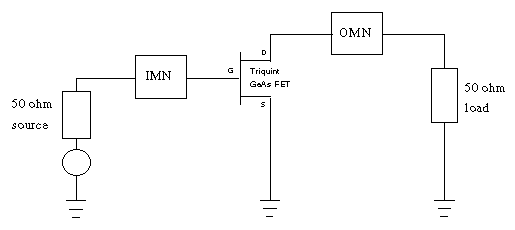
Figure 1: Block diagram of a FET amplifier
You are to design a single-stage amplifier using a transistor
that is conditionally stable at the design frequency of f
= 15 GHz. The process is outlined in the paper "A Deterministic
Approach for Designing Conditionally Stable Amplifiers",
authored by M. L. Edwards, S. Cheng, and J. H. Sinsky (IEEE
Transactions on Microwave Theory and Techniques, VOL. 43,
NO. 7, July 1995).
The core of the amplifier is a field effect transistor (FET) in
common-source configuration. In MDS, there is a built-in model
library for the Triquint GaAs (gallium arsenide) FET. This model
has parameters that define the bias level for the FET, so you
do not have to implement DC bias circuits. You may also
omit the coupling capacitors.
There is a 50 ohm source impedance on the input side of the FET
and a 50 ohm load on the output. To keep things simple, use ell
circuits (i.e., capacitors and inductors) instead of microstrip
to construct the input and output matching networks.
Jointly Matched Terminations Method
The basic task is to define a region inside the Gamma_s plane
such that any Gamma_s within this region automatically results
in a stable Gamma_L. The output stability circle is mapped into
the Gamma_s plane. Depending on the device parameters, this translates
into three different configurations (Figs. 4, 7, and 8 from the
Edwards, Cheng, and Sinsky paper). The upper bound on gains resulting
from jointly stable terminations is GMSM = 2*k*GMSG.
For GA -> 0, the constant gain circle overlaps
with the Smith chart unit circle. For GA ->
infinity, the constant gain circle overlaps the input stability
circle. Moreover, the centers of the input stability circle, unit
circle, and all the constant gain circles are collinear.
Procedure:
- Compute k (preferred: 0.5 < k < 1)
- Compute D1 = |S11|2
- |delta|2 where delta = S11S22
- S12S21
- Compute K1 = |C1|2
- D12 where C1
= S11 - (delta)(S22*)
- Compare your results against Figs. 4, 7, and 8 from the Edwards,
Cheng, and Sinsky paper. All conditions must be simultaneously
met; otherwise, this method cannot be used.
- Compute GMSM = 2*k*(|S21|/|S12|)
- Choose GA <= GMSM -
2 dB for design robustness (allowing for parameter variations).
- Draw the GA = const. circle.
- Choose Gamma_s on the GA = const. circle.
- Design the input matching network (IMN).
- Attach the IMN to the transistor and simulate/measure Gamma_OUT.
- Design the output matching network for Gamma_L = conjugate(Gamma_OUT).
Questions
- Figure 3.3.9 on page 228 in the Gonzalez textbook (2nd
edition) shows three different types of resistive loading configurations.
Which one provides the best compromise? Think of noise and output
power.
- For each of the following design methods, list some of their
advantages and disadvantages:
a) Resistive loading, b) Designing for GA,
c) Jointly matched terminations.
FET Characteristics
Assignment
In this section, you will determine the operating characteristics
of the Triquint FET.
Circuit construction

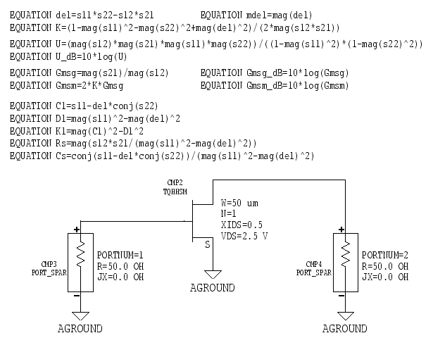
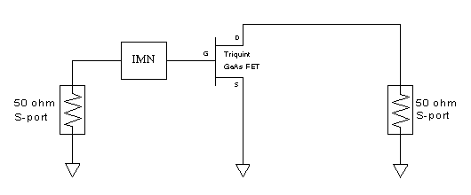
Figure 2: FET characterization test circuit
- Construct the circuit shown in Figure 2. To access the Triquint
FET, click [MB:INSERT/MDS COMPONENTS/TRIQUINT - HA/FET MODEL/LINEAR
HHSM].
Next to the FET symbol on the circuit page are four changeable
transistor parameters. W is the width of a single gate
finger and N is the total number of interdigitated gate
fingers. VDS and XIDS set the DC bias level for
the FET. VDS is the drain-source voltage. XIDS determines
the ratio of drain current to the maximum allowed drain current,
i.e. XIDS = IDS / IDSS.
For the test circuit, XIDS = 0.5 means that the drain-source
current is at half the maximum value.
Simulation & Output
- Configure MDS for an S-parameter simulation. Linearly
sweep the frequency from 1 to 21 GHz. Use a step size of 1 GHz.
In the 'Simulation Setup' window, define the equation variables
K, mdel, Gmsg_dB, Gmsm_dB, U_dB,
D1, K1, Rs, and Cs as output variables.
- When the simulation is finished, use the template method to
plot each S-parameter on its own Smith chart. On the same
presentation page, use a template to create a tabular listing
of the S-parameters versus the frequency. Finally, on the
same presentation page, add listing columns for frequency, K,
mdel, Gmsg_dB, Gmsm_dB, U_dB, D1,
K1, Rs, and Cs.
Items to turn in
- Turn in a printout of the FET characterization circuit.
- Submit a printout of the presentation page containing the
S-parameter plots, tabular listing, etc.
Questions
- At the design frequency of 15 GHz, verify that the Triquint
FET meets the requirements for using the jointly matched terminations
method. Which configuration (Fig. 4, 7, or 8 from the Edwards,
Cheng, and Sinsky paper) does the Triquint FET match?
- Comment on the magnitudes of S11 and S22.
What are the important characteristics of a FET that would cause
S11 and S22 to have such values?
Device Parameter Variation and Stability Boundaries
Assignment
You will examine how device parameter variation affects the input
stability circle and gain circle, which then impacts the choice
of Gamma_s and GA.
Parameter variations (sometimes as high as 20%) naturally occur
in the manufacturing process. Thus, not all devices are identical.
Accounting for this yields a more robust design. For this lab,
assume that the gate width of the FET can vary by 10% about its
nominal value of 50 um (micrometers).
Circuit construction

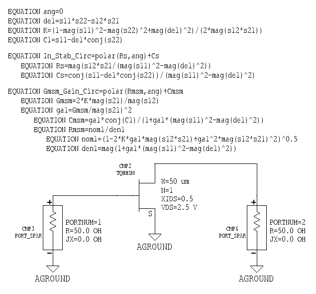
Figure 3: Device parameter variation test circuit
- Construct the circuit shown in Figure 3. This is essentially
the same circuit as in Figure 2, but the equations are different.
Record the component number (CMP#) of the FET; you will
need it later.
- In_Stab_Circ defines the input stability circle, while
Gmsm_Gain_Circ defines the maximum single-sided matched
gain circle.
Simulation & Output
- Configure MDS for an S-parameter simulation. In the
'Simulation Setup' dialog window, set Sweep type to "Single
Point". The frequency should be changed to 15 GHz.
- Click [Sweeps/control…] on the 'Simulation Setup' window
to get the 'Sweeps and Control' window. Select "Parameter
Sweep" and then click [OK]. The 'Simulation Setup' window
should now change its appearance to allow you to set up the parameter
sweep.
- Set Parameter Name to "ang". This is the
same as the equation variable ang (angle) on the circuit
page. Set Sweep type="Linear", Start=0,
Stop=360, and Step-size=5. The multipliers should
all be "x1.0". MDS will then sweep the ang variable
a full 360 degrees in 5 degree increments, which is used to plot
the input stability circles and gain circles.
- Click [Sweeps/control…] again to get the "Sweeps
and Control' window. In the subpanel labeled Apply this sweep/control:,
select "Parameter Sweep". In the subpanel labeled To
this simulation:, select "SWEEP:sweep1". Click [OK].
The Simulation Sequence panel on the left side of the parameter
setup window should look something like this:
SWEEP:sweep2
SWEEP:sweep1
SP:sim1
If you don't see the nested sweeps in the Simulation Sequence
panel, then you will need to try again.
- In Figure 3, the component number of the FET is CMP2.
Set Parameter Name to "cmp2.W" (use your own
CMP#). Set Sweep type="Linear", Start=45,
Stop=55, and Step-size=2. The multipliers should
all be "micro". MDS will then sweep the W (gate
finger width) variable of CMP2 from 45 to 55 um in 2 um
increments.
The net effect of the two-level nested sweep is this: For each
FET gate width (six values from 45 to 55 um), MDS will compute
the points needed to plot the input stability circle and gain
circle for the given W value.
- In the Simulation Sequence panel, click "SP:sim1"
to return to the standard 'Simulation Setup' dialog window. Define
the equation variables In_Stab_Circ and Gmsm_Gain_Circ
as output variables. Run the simulation.
- Once the simulation is done, create a Z-Smith chart on a new
presentation page. Plot the variables In_Stab_Circ and
Gmsm_Gain_Circ on that same Smith chart.
Items to turn in
- Turn in the Smith chart plot showing how the device parameter
variation affects the input stability circle and gain circle.
Questions
- Briefly explain the behavior of the stability and gain circles
as a function of the transistor's gate width.
Choosing Gamma_s
Assignment
Find the appropriate source reflection coefficient (Gamma_s) value
for a design frequency of 15 GHz and an available gain of GA
= GMSM - 2 dB (to allow for parameter variations).
Circuit construction

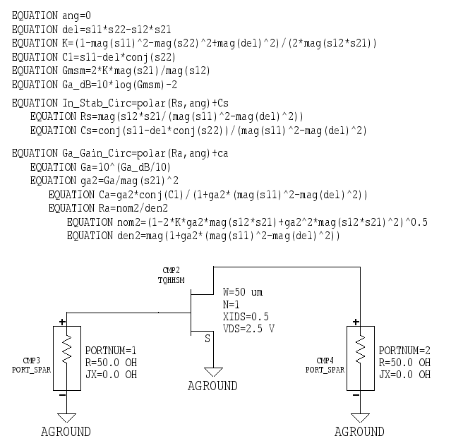
Figure 4: Gamma_s test circuit
- Construct the circuit shown in Figure 4. This is essentially
the same circuit as in Figure 3, but the equations are slightly
different.
- In_Stab_Circ defines the input stability circle, Ga_Gain_Circ
defines the constant available gain circle, and Ca is the
center of the constant gain circle.
Simulation & Output
- Configure MDS for an S-parameter simulation. In the
'Simulation Setup' dialog window, set Sweep type="Single
Point" and Frequency=15 GHz.
- Set up a 0 to 360 degree parameter sweep on the ang
equation variable (just like the previous section). The step size
should be 1 degree for better resolution. The is just a one-level
sweep, so the FET's gate width should initially be fixed at 50
um (do not sweep W).
- Define the equation variables In_Stab_Circ, Ga_Gain_Circ,
and Ca as output variables. Run the simulation.
- After the simulation is complete, create a new presentation
page and plot the output variable In_Stab_Circ on a Z-Smith
chart. Add Ga_Gain_Circ as a trace on the same Smith chart.
Add Ca as another trace on the same Smith chart.
- In this step, you will draw a line on the presentation page
that connects the center point of the Smith chart to the center
point Ca of the constant gain circle.
Choose [MB:INSERT/LINE/SOLID/.01"]. Position the mouse pointer
directly over the center of the constant gain circle (where the
Ca point is located). Click the left mouse button, hold
it down, and drag the mouse until the pointer is directly over
the center of the Smith chart. When you release the mouse button,
MDS will draw a line connecting the two points. If the line does
not quite go through the desired points, just delete the line
and try again.
- The desired Gamma_s value occurs at the intersection between
the line and the boundary of the constant gain circle. Use the
intersection point that is closest to the center of the Smith
chart. To make reading the Gamma_s value more accurate, insert
a marker on the constant gain circle trace.
Select [MB:INSERT/MARKER ON TRACE]. A message window appears that
says "Select trace and drag marker to the desired location".
Click the Ga_Gain_Circ circle, hold down the left mouse
button, drag the triangular marker to the intersection of the
circle and the line, and release the mouse button. A data box
then tags along with the mouse pointer. Place the box where you
want it to go and click the mouse button to drop it onto the presentation
page.
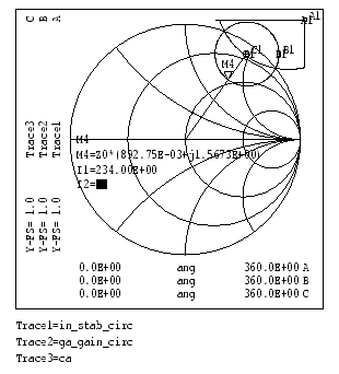
Gamma_s will be given by an expression such as "M4=Z0*(a+jb)",
where M? is the marker ID, Z0 is the 50 ohm characteristic
impedance, and a and b are the real and imaginary
parts of Gamma_s.
Tip: You can get a more accurate Gamma_s value if you zoom
into the presentation page so that the gain circle fills most
of the screen.
Refer to Figure 5 for an example of what your finished plot should
look like.

Figure 5: Sample Smith chart with circles and added
line
IMPORTANT: Repeat the simulation and output procedures
at the extremes of the FET gate width, i.e. at W = 45 um
and W = 55 um. Determine the corresponding Gamma_s value
at each gate width.
Items to turn in
- Submit printouts of the W = 45 um, 50 um, and 55 um
Smith charts.
Questions
- What are the individual Gamma_s values (magnitude & phase)
at W = 45 um, 50 um, and 55 um?
- Calculate the average Gamma_s and compare it to the value
of Gamma_s at W = 50 um.
Designing the IMN
Assignment
You will design the input matching network (IMN) of the amplifier.
Circuit construction

Figure 6: IMN test circuit
- Construct the circuit shown in Figure 6. The FET bias parameters
are unchanged.
When designing the IMN, use the average value of Gamma_s you computed
in the previous section. Build the IMN using ell circuits.
Tip: The performance of the amplifier is dependent on the
accuracy of the IMN's component values. To get better results,
you may wish to test the IMN by itself first. Use MDS's optimization
feature to tune the IMN (just like Lab 3 from Microwave Circuits
I).
Simulation & Output
- Configure MDS for an S-parameter simulation. In the
'Simulation Setup' dialog window, set Sweep type="Single
Point" and Frequency=15 GHz. For the circuit in Figure
6, Gamma_OUT = S22.
- After the simulation is completed, create a new presentation
page and add a listing column to view the value of S22.
IMPORTANT: Perform the simulation and output procedures
at W = 45 um, 50 um, and 55 um. Determine the corresponding
Gamma_OUT values at each gate width.
Items to turn in
- There is nothing to turn in.
Questions
- What are the individual Gamma_OUT values (magnitude &
phase) at W = 45 um, 50 um, and 55 um?
- Compute the corresponding transducer gain GT
for each value of Gamma_OUT.
- Calculate the average Gamma_OUT and compare it to the value
of Gamma_OUT at W = 50 um.
Designing the OMN
Assignment
You will finish the amplifier circuit by designing the output
matching network (OMN).
Circuit construction

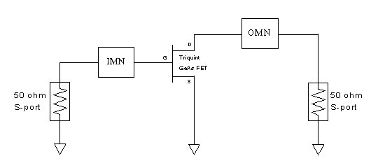
Figure 7: Final amplifier circuit
- Construct the circuit shown in Figure 7. The FET bias parameters
are unchanged.
When designing the OMN, the load reflection coefficient Gamma_L
is given by the expression Gamma_L = conjugate(Gamma_OUT). Use
the average value of Gamma_OUT that you computed in the previous
section. Build the OMN using ell circuits.
Tip: To achieve better results, consider testing the OMN
by itself first. Use MDS's optimization feature to tune the OMN.
Simulation & Output
- Configure MDS for an S-parameter simulation. Linearly
sweep the frequency from 12 to 18 GHz. Use a step size of 0.25
GHz.
- After the simulation is over, create a tabular listing of
the S-parameters on a new presentation page.
Items to turn in
- Turn in a printout of your final amplifier schematic. If you
used subcircuits for the matching networks, then include printouts
of those, too.
- Turn in a printout of the S-parameter tabular listing.
Questions
- What is the gain at the design frequency? Does it meet the
design requirements (to within 2 or 3 percent)?
- Compare the magnitudes of S11 and S22
in the amplifier circuit with matching networks to their corresponding
values with no matching networks.
