Description:
In a similar setup to scanning electon microscopes, an electron beam scans across the substrate surface and exposes electron sensitive coating. A grid of pixels is superimposed on the substrate surface, each pixel having a unique address. The pattern data is transfered to the controling computer, which then directs the electron beam as to realize the pattern on the substrate pixel by pixel. The electron beam used is either a Guassian round beam or Variable Shaped Beam (VSB). There are two methods of scanning the beam over the substrate surface to write the pattern data. With raster scan, the electron beam is scanned across lines of pixels and the wafer is shifted to the next line. With vector scan, an area of an individual chip is selected, and the beam draws out the features in that area one-by-one.
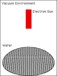
Diagram of a basic electron beam lithography setup.
Advantages:
- Computer-controlled beam
- No mask is needed
- Can produce sub-1 µm features
- Diffraction effects are minimized
- Electron beam can detect surface features for very accurate registration
Disadvantages:
- Swelling occurs when developing negative electron beam resists, limiting resolution
- Expensive as compared to light lithography systems
- Slower as compared to light lithography systems
- Forward scattering in the resist and back scattering in the substrate limit resoution
Electron Beam Resists:
These are materials which exhibit changes, whether physical or chemical, due to exposure to a high-energy electron beam. Most electron beam resists are polymer chains. Some optical resists can also be used.
Positive Resists
Positive electron beam resists break down into less complex fragments on exposure to an electron beam. Because the less complex fragments have a lower molecular weight, they are more soluable by the developer than the unexposed resist.
Negative Resists
Negative resists form complex molecular links when exposed to the electron beam, and so become insoluable in the original solvent, which removes the unexposed resist.
Certain inorganic resists can also be used. A layer of GeSe onto which AgSe has been evaporated, acts as a negative resist. When exposed to the electron beam, the GeSe layer is filled with AgSe, and the combination can then be developed.