The Design
of a
Relay-Based Computer
Harry H. Porter III, Ph.D.
Portland State University
November 15, 2007
Table of Contents
What is a Relay?
Representing Binary Values
The “NOT” Circuit
The “OR” Circuit
An “AND” Circuit
A 1-Bit Logic Block
The Aritmetic Logic Unit (ALU)
Addition
Konrad Zuse’s Full Adder Circuit
The Increment Circuit
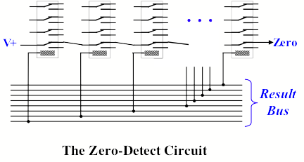
The Zero-Detect Circuit
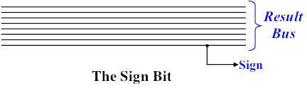
The Sign Bit
The Data and Address Busses
The Enable Circuit
LEDs
The Shift-Left Operation
3-to-8 Decoder
The Structure of the ALU
Register Storage
Feedback and Oscillation
Fixing the Register Circuit
Register Timing
Differences With the “As-Built” Register Circuit
Register Control
The Address Bus
Overall System Architecture
Physical Organization of Major Functional Units
The Arithmetic Logic Unit
The Register Unit
The Program Control Unit
Main Memory
An Example of Instruction Execution
The Clock Circuit
The Finite State Machine
The Timing of an Instruction
Instruction Decoding
Longer Instructions
The Instruction Set
MOV-8: The 8-Bit Move Instruction
ALU: The ALU Instructions
SETAB: The Load Immediate Instruction
INC-XY: The 16-Bit Increment Instruction
LOAD: The Load Instruction
STORE: The Store Instruction
MOV-16: The 16-Bit Move Instruction – General Form
MOV-16: The Halt Instruction
MOV-16: The Return / Branch-Indirect Instruction
GOTO: The Goto Instruction – General Form
GOTO Variant: The SETM Instruction
GOTO Variant: The JUMP Instruction
GOTO Variant: The CALL Instruction
GOTO Variant: The BNEG (Branch-If-Neg) Instruction
GOTO Variant: The BNC (Branch-If-No-Carry) Instruction
GOTO Variant: The BZ (Branch-If-Zero) Instruction
GOTO Variant: The BNZ (Branch-If-Not-Zero) Instruction
Assembly Language / Assembler
An Example Program
Parts List and Costs
Concluding Remarks
Introduction
This paper describes the design of a computer that I built out of relays. The computer, which was completed in 2005, is documented at
www.cecs.pdx.edu/~harry/Relay
which contains a number of photos and videos.
What is a Relay?
Inside every relay is an electromagnet. An electromagnet is simply a coil of wire, wound around an iron core. When electricity passes through the coil, a magnetic field is created and when the electricity is disconnected, the magnetic field collapses.
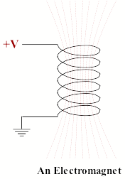
In every relay, there is a small switch situated next to the electromagnet. When electricity passes through the coil, the magnetic field moves the switch into one position. When the electricity is removed, a spring pulls the switch back into the other position. A relay consists of an electromagnet that operates a nearby switch.
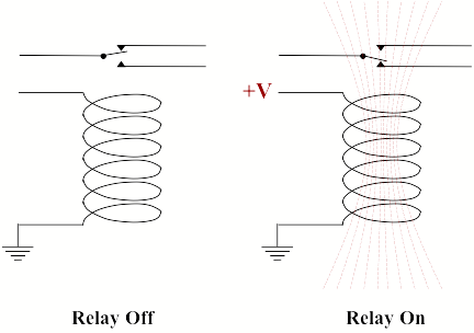
A double-throw switch has three contacts. In one position the movable contact makes a connection with a second contact, while in the other position the movable contact makes a connection with the third contact. Double-throw switches are also called on-on switches.
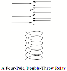
The relays used in this computer have, not one, but four identical switches located next to the electromagnet. When on, the electromagnet operates all four switches in unison. Each switch is a double-throw switch. For this reason, the relay is called a four-pole, double-throw relay.
All the relays used in this computer are the identical part, which is pictured below. The relays are 12 volt relays and the computer is powered with 12 volts DC. (Relays do not work with AC current.)
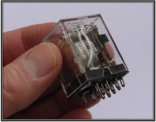
Incidentally, the term “computer bug” originated when a program failure was found to be caused by a moth, which had gotten caught between two contacts in an early relay-based computer. As you can see, these relays have a plastic cover, which makes this computer completely immune to “bugs.”
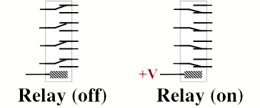
In designing the circuits used in the computer, I invented the following
schematic diagram to represent a relay.
Normally, relays are drawn in the “off” position, but sometimes it helps in understanding a circuit to portray some relays in the “on” position.
Notice that only one connection to the coil is shown. The assumption is that the second connection is to ground. For all the relays in this computer, one terminal of the coil is always connected to ground.
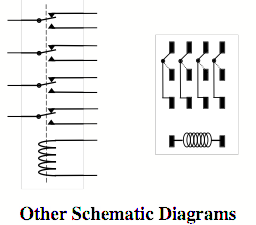
Here are some other schematic representations. The diagram on the left is the traditional notation. The diagram on the right is convenient since it shows the positions of the external connections.
Representing Binary Values
We represent a logical “1” with a connection to 12 volt power, symbolized as +V. A logical “0” is represented with “no connection to power.” Note that this is different than saying “0” is a connection to ground.
A wire that is not connected to power will essentially be at zero volts. If such a wire is connected to another relay coil or to a light, then any voltage charge on the wire will quickly fall to zero as the electricity bleeds out through the relay or light. And if the wire is truly unconnected to anything else, then we really don’t care what voltage charge it carries.
The relay is a robust, resilient device when compared to transistors or integrated circuits. In the design of this computer, concepts like charge, current, capacitance, resistance and inductance can be pretty much ignored. This is an electric computer, not an electronic computer. All that matters is whether there is a path to +V or not. It is very much a “logical” design, not an electronic circuit.
The “NOT” Circuit
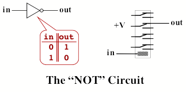
Here is a circuit implementing the logical “NOT” function with a single relay.
With an input of “0”, the relay will be off, as shown, and the output will be connected to power, which means the output will be “1.” An input of “1” will cause the relay to turn on, which will break the connection to power and cause the output to be “0”.
The “OR” Circuit
Here is a circuit implementing the logical “OR” function, using two relays:
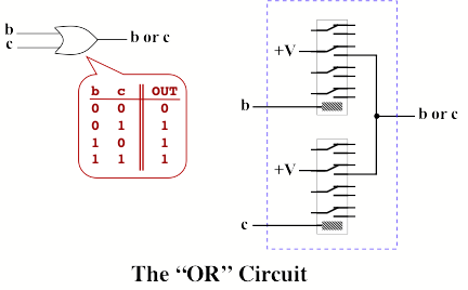
You might suggest the following “optimized” version of the “OR” circuit, which I call the “wired-OR” circuit. Since each input is either connected to power or unconnected, tying them together will mean that the output is connected to power if either of the inputs is.
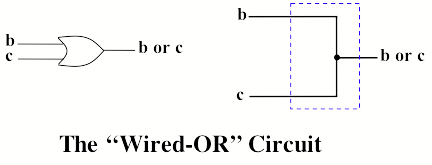
The wired-OR circuit will work in some situations, but will not work properly in every situation. Below is an example where the wired-OR circuit will produce the wrong result.
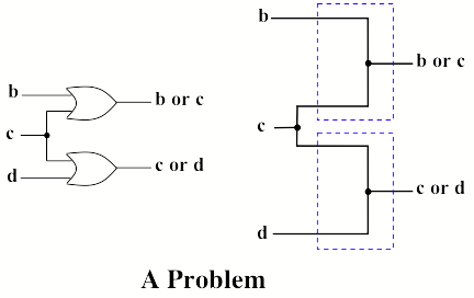
To see the problem, imagine that inputs “b” and “c” are “0” and input “d” is “1”. The “b or c” output should be “0” and the “c or d” output should be “1”. Unfortunately, there is a path from power (coming in through “d”) to the “b or c” output. Therefore, the “b or c” output will be “1”, which is incorrect.
The problem is that a signal can travel both directions along a wire. In this case, the “c or d” circuit is driving its “c” input high, and this has repercussions in the “b or c” circuit. Whenever a wire is meant to carry a signal in one direction, but some circuit can send a signal in the reverse direction, I say that “backfeed” or “backflow” can occur along the wire.
In some cases, backfeed will not cause any problems; in other situations it will cause other circuits to malfunction. The wired-OR is much simpler than using relays, so I prefer to implement the “OR” function by tying wires together, whenever it can be done without backfeed causing another circuit to malfunction.
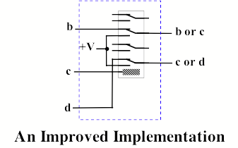
Below is a circuit that solves this problem and implements the desired functionality.
This circuit will work, but when using it we must remember that backfeed along
the “b or c” output will cause backfeed along the “b” input. Also, backfeed along the “c or d”
output will cause backfeed on the “d” input.
An “AND” Circuit
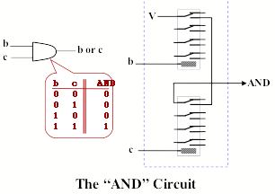
Here is an implementation of the logical “AND” gate, using two relays. This
circuit is not affected by backfeed.
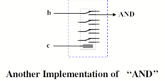
Below is another implementation of “AND”, but backfeed can occur in this
circuit. In particular, backfeed
on the output can cause backfeed on the “b” input.
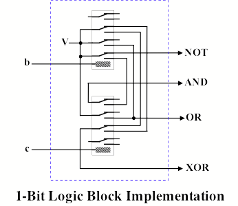
A 1-Bit Logic Block
The “1-Bit Logic Block” implements four logic functions at once. It produces four outputs, providing the logical AND, OR, NOT, and XOR functions.
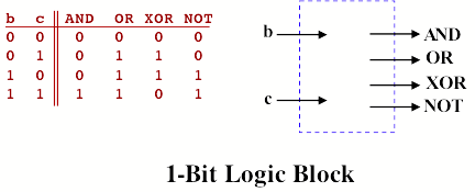
The following circuit implements these functions in such a way that backfeed cannot occur.
The Aritmetic Logic Unit (ALU)
Using the 1-bit logic circuit shown above, we can start to construct an Arithmetic Logic Unit (ALU). This computer is an 8-bit computer, and works most easily with byte-sized quantities. Consequently, the ALU takes as inputs, two 8-bit values and produces an 8-bit result. The ALU is capable of computing several different operations on the two inputs, so another input controls what operation is performed by the ALU.
In this computer, the two inputs to the ALU are called “B” and “C.” Both inputs are 8 bits. The output of the ALU is called the “Result” and is also 8 bits. Within a byte, the bits are numbered from 0 to 7, with bit 0 being the least significant.
Thus, the inputs to the ALU are:
B = b7 b6 b5 b4 b3 b2 b1 b0
and
C = c7 c6 c5 c4 c3 c2 c1 c0
The most basic functions that can be computed are logical AND, OR, XOR, and NOT. For example to compute AND, each of the 8 bits of one input is ANDed with the corresponding bit from the other input to produce a single bit of the output. Note that the NOT function depends only on the B input.
The ALU contains eight 1-bit logic blocks (as described above), which compute logical AND, OR, XOR, and NOT on all 8 bits, as shown in the 8-bit logic circuit below.
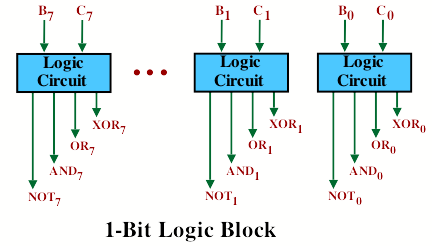
The logic circuit computes
B AND C
B OR C
B XOR C
NOT B
This ALU can also compute
B + C (addition)
B + 1 (increment)
B << 1 (shift left)
Addition
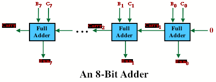
The ALU is capable of adding two 8-bit numbers. Each bit is added using a “full adder” circuit. Eight full adders are chained together to form an 8-bit adder.
Recall that a full adder takes two bits, adds them and produces a 1 bit result. Furthermore, a full-adder takes a “carry input” from the previous stage to the right and produces a “carry output” to the next stage to the left.
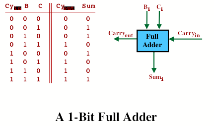
By connecting 8 full adders together, feeding the “carry output” from one into the “carry input” of the next, we can build an 8-bit adder. We feed a “0” into the “carry input” of the least significant bit. When adding two 8-bit numbers, the result will sometimes overflow into the 9th bit; this bit is simply the carry out from the most significant full adder.
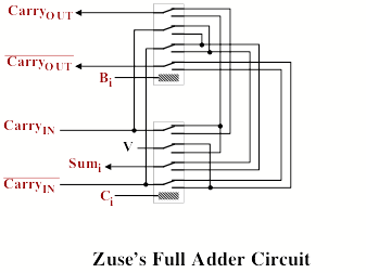
Konrad Zuse’s Full Adder Circuit
The full adder circuit used in my computer was invented by Konrad Zuse for his Z3 computer. The Z3 was built out of relays and completed in 1941, in wartime Berlin. This was no small feat, since money for such pure research projects was hard to come by in the middle of World War II. It is reasonable to refer to Zuse’s machine as the first functional computer, since all previous “computers” were mechanical calculators.
Except for the full adder, I designed all circuits used in my computer.
The full adder circuit uses two wires, instead of one, for each carry. This “dual rail” design sends the carry along in both negated and non-negated form. [For an interesting online simulation, see http://tams-www.informatik.uni-hamburg.de/applets/hades/webdemos/05-switched/20-relays/zuseadd.html ]
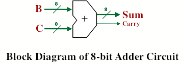
We can summarize the 8-bit adder circuit with the following block diagram.
The diagonal marks on the “B” and “C” inputs and on the “Sum” output indicate that there are 8 parallel lines, one for each bit. We also see the “carry output” from the leftmost (i.e., most significant) stage of the adder.
The Increment Circuit
For normal addition, we supply two 8-bit operands to the adder and we supply a “0” for the carry input to the rightmost (i.e., least significant) stage. Using the dual rail carry design of Konrad Zuse, this means we must supply a “1” for the negated carry input to the least significant first stage.
The ALU is also capable of incrementing B.
Incrementing can be implemented very easily, using the adder, as follows: ignore C and supply a “1” as the carry input to the least significant stage. Since we use the dual rail carry design, we must supply “0” as the negated carry input to the rightmost stage.
The Zero-Detect Circuit
The ALU is also capable of detecting when the result is all zeros. The following circuit samples the 8 bit result. When the value on the result is 00000000, all 8 relays will be off and the zero detect output will be “1”. However, if any bit in the result is “1”, then the corresponding relay will turn on, and the path from “V” to the output will be broken.
The Sign Bit
Computers represent negative integers using two’s complement representation. Whenever a number is negative, the most significant bit will be “1”. The ALU can detect the sign of the result by simply pulling off the sign bit. No relays are necessary.
The Data and Address Busses
A single wire can carry a single bit. A “bus” is simply a set of several parallel wires which can carry several bits at once. This computer contains two important busses, the “data” bus and the “address” bus.
The data bus is 8-bits wide, so the data bus transfers a byte at a time.
DATA
BUS = d7 d6 d5 d4 d3 d2 d1 d0
The rightmost bit (d0) is the least significant bit.
The address bus is 16-bits wide, so the address bus transfers two bytes at a time.
ADDR
BUS = a15 a14 a13 a12 a11 a10 a9 a8 a7 a6 a5 a4 a3 a2 a1 a0
The rightmost bit (a0) is the least significant bit.
The data bus is used to transfer data and instructions between main memory, registers, and the ALU. The address bus is used primarily to deliver addresses to the main memory.
The Enable Circuit
From time to time it is necessary to connect a group of 8 wires to another group of 8 wires. For example, we have an 8-bit “data bus” and we may wish to gate some particular value onto the bus. We can perform this gating operation with the “enable circuit.”
The enable circuit is controlled by a single line. When high, it connects the 8 wires to the bus. When low, the 8 wires are isolated.
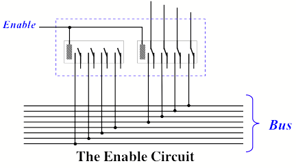
For example, the 8-bit logic block produces the following values:
B AND C
B OR C
B XOR C
NOT B
At times, we are interested in the XOR value, so we’ll need to be able to gate it onto the result ALU result bus.
LEDs
The enable circuit diagram also shows eight lights. This computer employees a number of lights to visibly monitor its operation. In the above diagram, the lights always reflect the XOR result, regardless of whether that value is subsequently gated onto the result bus.
For simplicity, I use the schematic symbol for a light in the diagrams instead of the symbol for a LED (light emitting diode). The computer actually contains red LEDs. Normally, an LED is used in series with a resistor. The LEDs used in this computer each contain a small built-in resistor, so they can be connected directly between power and ground, like any normal light bulb. (Details about the part numbers and costs of the components is given later in this document.)
The LEDs are all connected in the same way: one terminal is connected to ground and the other is connected to some wire of interest.
Obviously, the LEDs have no impact on computation: they simply make visible the state of some wire without changing anything. The computer would work identically with no LEDs. However, the LEDs form the only output of the computer: without LEDs, it would be impossible to retrieve any result.
Typical programs for this computer work as follows: some input values are preloaded into registers and then the computer begins executing. Upon completion of a computation, the program leaves the result(s) in some register(s). The state of the register(s) can be seen from the LEDs.
LEDs are also used to monitor the state of various control connections. The LEDs were critical in debugging the wiring during construction; without these LEDs, it would have been virtually impossible to find errors and understand what was happening.
The LEDs also make the computer interesting to watch while it is computing, although it is pretty much impossible to interpret the flashing lights. One exception is the “program counter”; you can follow the instruction execution walking through memory and occasionally branching by watching the value in the program counter (PC) register.
The Shift-Left Operation
Our ALU is also capable of shifting the 8-bit value “B” left by one bit. The shift is circular, which means that the most significant bit is shifted into the rightmost (i.e., least significant) position.
In the following diagram, we show how B can be shifted left and placed on the Result Bus. Whenever the enable control is low, B is isolated from the result. When high, the bits of B are connected to the result, after begin shifted.
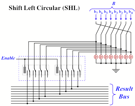
Sometimes a circular shift is called “rotate”. This computer can only shift by one bit and cannot shift right, but notice that you can achieve the effect of shifting right by one bit by shifting left 7 times. Therefore, a single “shift left” instruction is included in the instruction set, since any other shift amount can be achieved with up to 7 repetitions of the instruction.
Also, it is sometimes the case that one would like to shift in zero, rather perform a rotate. This too is possible but requires extra instructions. For example, to shift left (bringing a “0” into the rightmost position, instead of rotating), you could first perform the rotation and then clear the least significant bit using the logical AND operation with the value 11111110.
This reveals an important principal behind the design of this computer: I have included enough to make it fully programmable and even reasonably usable, at the cost of requiring a few extra instructions. For example, any desired shifting or rotating can be accomplished with the single shift operation provided, along with the logical operations. As another example, the ability to subtract was not included directly, but it is straightforward to perform subtraction using addition. The algorithm is to simply negate the second value first, and then add. While there is no negation operation, negating an integer can be done by first complementing it (i.e., performing the logical NOT) and then incrementing it. Since both NOT and INCREMENT are instructions, subtraction can be done using NOT, INCREMENT, and ADD operations.
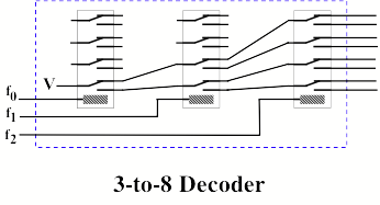
3-to-8 Decoder
A 3-to-8 decoder takes 3 bits of input and produces 8 bits of output. With 3 inputs, there are 23, or 8, possible input values. The output is “1 hot”. In other words, all output are low except for a single line, and the inputs are used to select which output line is to be high.
Other computers also use 2-to-4 decoders, 4-to-16 decoders, and so on. In general, with N inputs, a decoder will have 2N outputs.
Here is a simple circuit implementing a 3-to-8 decoder.
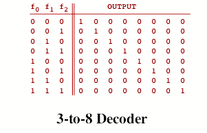
The ALU takes 3 control lines telling which operation to perform, according to this table:
f0 f1 f2
0 0 0 ADD
0 0 1 INCREMENT
0 1 0 AND
0 1 1 OR
1 0 0 XOR
1 0 1 NOT
1 1 0 SHIFT LEFT
1 1 1 < not used >
These 3 lines are labeled with “f” since they are called the ALU “function code”. The ALU function code inputs enter the ALU and go straight into a 3-to-8 decoder to determiner which operation is selected.
The last function code value (111), which is labeled <not used>, is supplied when the ALU is not being used. When 111 is supplied, the ALU result output will be all zeros, i.e., unconnected. Since the output result from the ALU is connected directly to the computer’s data bus, the <not used> function code is necessary to ensure that the ALU does not put some value onto the data bus when the data bus is being used for some other purpose.
[In retrospect, it was a mistake to assign the function code 111 to <not used>; it would have been a better decision to assign 000 to <not used>. The reason is that it is convenient at times to turn off portions of the computer’s control circuitry, which causes the ALU function control to be 000. Unfortunately, this causes the data bus to be driven by the ADD circuitry in the ALU, rather than to be quiescent. If 000 had been the <not used> function code instead, then whenever the control circuitry was not driving the ALU function inputs, the ALU result would be unconnected to the data bus.]
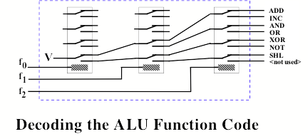
The Structure of the ALU
The next figure shows the complete design of the arithmetic logic unit (ALU).
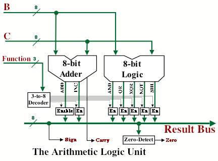
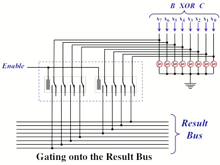
The 3 function code control lines go into a 3-to-8 decoder. The <not used> output is not connected, but the other 7 outputs from the decoder are each attached to an enable circuit. Each enable circuit can gate its output directly onto the 8-bit result bus. For example, when the function control input is 011, the output of the ALU is required to be “B OR C”. The enable circuit connected to the OR output from the 8-bit Logic Circuit is turned on, which gates the OR value onto the result bus, as required.
When all of the 7 enable circuits are inactive (i.e., when the function code is 111 <not used>), the result bus is unconnected.
The ALU also takes two inputs of 8-bits each, called “B” and “C”. The B and C inputs are fed into the 8-bit logic circuit and the AND, OR, XOR, and NOT values are all computed. The shift left (SHL) output is included in the 8-bit logic circuit but recall that it does not include any relays and is really nothing more than a routing of the B lines, with the one-bit rotation.
The B and C inputs are also directed into the 8-bit adder circuit. In this diagram, we show the adder as producing the sum (for ADD) and the B+1 (for INC), although this is not exactly right. There is a little circuitry not discussed here that uses the single 8-bit adder to perform either B+C or B+1.
The ALU also produces “sign”, “carry”, and “zero” outputs.
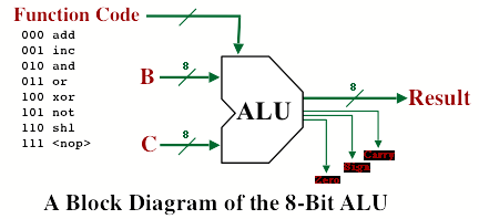
We can summarize the computer’s ALU with the following block diagram.
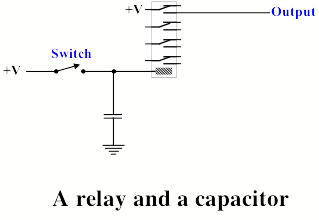
Register Storage
Next, take a look at the following circuit.
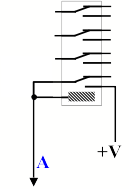
If line “A” should ever go high, this relay will turn on. However, if “A” is subsequently disconnected to whatever was driving it, the relay will stay on, due to the feedback loop from power through the relay’s switch to its coil. So this relay forms a simple memory, capable of latching a single bit. Once turned on, it stays on.
This circuit forms the basis of the design of the registers used in this computer. We’ll call it a “bit relay”, since it can store a single bit.
As this circuit is drawn, the bit relay will stay on forever, until the power is cut off. To hold the value, we’ll keep supplying power; to clear the bit, we’ll cut the power.
Next, let’s put eight bit relays together to create an 8-bit register.
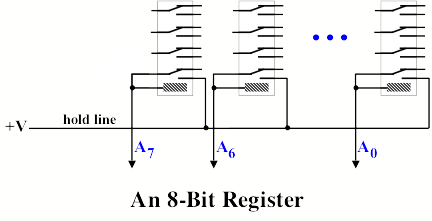
The relays in the register are numbered from 0 (on the right) to 7 (on the left). Bit 0 is the least significant bit and 7 is the most significant bit, which follows the “big endian” bit ordering.
For now, the “hold line” is connected to power, so that once loaded, the register will retain its value. To clear the register, we’ll cut the power to the hold line.
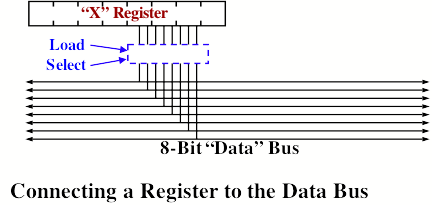
The next step is to get the data out of the register and onto the data bus.
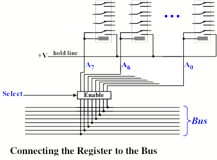
The control line labeled SELECT is used to “read out” the register’s value. When SELECT is high, the value stored in the register will be gated onto the bus. In other words, when a register is selected, it drives the bus, and the 8-bit value stored in the register is made available to other parts of the computer by being placed on the bus. When not selected, the register is isolated from other parts of the computer.
Now let’s ask how a value can be loaded into the register from the bus. Notice that when the register is selected, each bit is connected to the corresponding line of the bus. If nothing else is driving that bus line, then the relay, if on, will drive the bus line. But also notice that if the bit relay happens to have been off, but something else is driving the bus line, the bit relay will get turned on. And once on, the bit relay will latch and remain on until power to the hold line is removed.
To store a value into a register, we want to first cut the power to the hold line, thereby clearing the register to all zeros, and then we want to turn the enable circuit on, which will load the register with whatever value is on the bus.
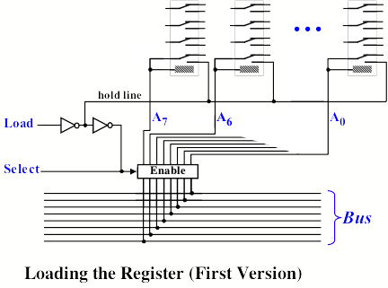
To understand this circuit, imagine that initially both LOAD and SELECT control lines are low. Therefore the enable circuit is off and the register is not connected to the bus. The output of the first NOT gate is HIGH, so power is supplied to all the bit relays, via the hold line. Since power is delivered to all the bit relays, the register will retain whatever value it already contains.
Now, imagine that the LOAD control line transitions to high. As the signal propagates through the first NOT gate, the power to all the bit relays will be cut and all the bit relays will turn off. Also the second NOT gate will change and the output from it to the enable circuit will go high. Next, the enable circuit will turn on and the bit relays will each be connected to the bus. Next, some of the bit relays will turn on, depending on whatever value is on the bus.
Next, imagine that the LOAD control line goes back to low. As the change propagates through the first NOT gate, the hold power to the bit relays will be restored. This will cause the bit relays to latch and retain whatever value was on the bus. It will also cause the second NOT gate to change, which will subsequently cut power to the enable circuit. This will, in turn, disconnect the bit relays from the bus.
To recapitulate, when LOAD goes high, the register is momentarily cleared and then subsequently, the register is loaded from the bus. Then, on the falling edge of LOAD (when LOAD returns to low), the value in the register is latched, as the register is disconnected from the bus.
Note that there are some subtleties related to timing. The register circuit is the only circuit in the computer that is “edge sensitive”, so we need to discuss it in more detail.
First, imagine that the LOAD line is low. Recall that a NOT circuit consists of a single relay. If the input is low, the relay is off; if the input is high, the relay is on. The relay in the first NOT circuit is initially off. The relay in the second NOT circuit is initially on, since its input is high.
When LOAD goes high, the relay in the first NOT will turn on. After this happens, the relay in the second NOT circuit will begin to turn off. At the same time, any bit relays which were previously on, will also begin to turn off. It will take some time for all these relays to turn off, but they will all turn off at roughly the same time. Only after the relay in the second NOT has turned off, will the enable circuit begin to turn on. As the enable circuit turns on, the relays in the enable circuit will be switched on. This will also take some additional time, which will allow all the bit relays to finish turning off, in case any one was a little slower than the others. By the time the enable circuit relays have turned on, all the bit relays will have been given enough time to turn off.
Then, some of the bit relays will turn back on.
Next, imagine what happens when the LOAD line goes back to low. The relay in the first NOT circuit will turn off. Once this is complete, the power to the bit relays will be restored and whatever value they contain will be latched. Then the relay in the second NOT circuit will turn back on, which will take a little time. Once on, the relays in the enable circuit will turn off. So you can see that the enable circuit can not disconnect the bit relays from the bus until after the hold power to the bit relays is restored.
There is one error in this design, as presented so far. Imagine that register Y is being loaded from the bus and that Y’s LOAD line has just gone high. First, power to the hold line is cut. Then the enable circuit turns on and some of the bit relays in Y are switched on. Unfortunately, power can flow back from whatever bit relay comes on, along the hold line, and change the input to the second NOT circuit. The second NOT gate will then switch and power to the enable circuit will immediately be cut. After the enable circuit turns off, the bit relays will be disconnected from the bus and, without any power to drive the hold line, the bit relays will all switch off. Furthermore, the second NOT gate will again switch.
Feedback and Oscillation
At this point, the register circuit (as designed) will begin oscillating, with relays flipping on and off as fast as they can. This is bad and will cause the relays to act like buzzers. Here is the simplest circuit with oscillating feedback.
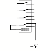
When this relay is off (as shown), power will be supplied to the coil, causing
it to turn on. When the relay is
on, power will be disconnected from the coil, causing it to switch off. The relay will oscillate as fast as it
can, making a buzzing sound. The
relays used here are rated for a maximum switching speed (5 cycles per second)
and when buzzing, they will overheat and fail.
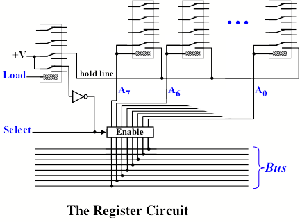
Fixing the Register Circuit
When I first designed the register circuit, I came up with the design presented above. I believed it would work but fortunately I built a 3-bit prototype to test the design, before building more. It was at this point that I discovered the possibility of feedback and oscillation, as discussed above.
It is important to build prototypes, but it is a matter of experience and wisdom to know when it is wise to bother with a prototype and when it is more practical to go ahead and build the final version without prototyping first.
The fix to the circuit is simple; we just need to make sure that power coming back through the hold line can’t act as input to the second NOT gate. In the basic design of a NOT gate, only one switch in the relay is used; in the following modification, we are using two switches in the relay, in order to isolate the hold line from the second NOT gate.
Register Timing
When loading a register, we assume that the value on the bus is stable and unchanging before the LOAD line goes high and that the bus remains unchanging until well after the LOAD line goes low.
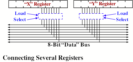
Imagine that we have several registers connected to the data bus, each with its own LOAD and SELECT lines. Using the bus, we can transfer data from one register to another. For example, to transfer a value from register X to register Y, we should raise X’s SELECT line and raise Y’s LOAD line.
In the following timing diagram, we see the SELECT line to register X and the LOAD line to register Y going high on the same clock edge. The LOAD line goes low on the next edge, but the SELECT line stays high for 2 units of time, to ensure that the bus remains stable until well after Y’s LOAD line goes low.
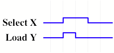
We can raise X’s SELECT line and Y’s LOAD line on the same clock edge, since we
don’t care what order these control lines go high. If X’s select line goes high first, then X’s value will be
out on the bus early. Later, Y
will cleared to all zeros and then connected to the bus. Y will load the correct value. On the other hand, if Y’s LOAD line
goes high first, then Y will be cleared and then connected to the bus, which is
still all zeros. Then, when X’s
SELECT line goes high sometime later, its value will be gated onto the
bus. This will cause the bit
relays in Y to change at that later time, but Y will still be loaded with the
correct value.
However, we must make sure that X’s SELECT line stays high during the trailing edge of Y’s LOAD line. If we were to drop both X’s SELECT and Y’s LOAD on the same clock edge, we could have a race problem in which X’s enable circuit disconnected X’s value from the bus before power was restored to Y’s bit relays. If this occurred, some bit relay in Y might turn off in the instant before power was restored and a bit might not get latched.
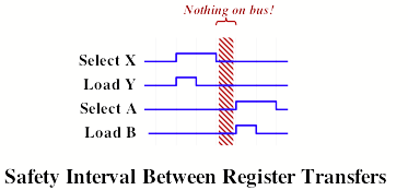
Also note that in our register design, we must never have two registers simultaneously selected onto the bus. Imagine that some register—say register X—is selected onto the bus and imagine that for some reason, some bit which is low in X suddenly goes high on the bus, perhaps because some other register is simultaneously selected. This high value from the bus line will flow back through X’s enable circuit and will turn the corresponding bit relay in X on. Thus, the value in X would be changed, even though X’s LOAD line never went high. So in our design, a register is somewhat “vulnerable” when selected.
To make sure this doesn’t happen, we will always leave a full clock cycle as a “safety interval” between any two SELECT lines going high. This ensures that we can never have two different values simultaneously gated onto the bus, risking data corruption.
The next diagram shows how closely we can space two distinct register transfers.
Differences With the “As-Built” Register Circuit
In the register design presented here, each register uses a single enable circuit. This enable circuit is active both when the register is selected and when the register is loaded.
If, for any reason, two registers should be simultaneously selected, then bits would be turned on erroneously. In fact, whenever two registers are selected at the same time, their values will be modified by turning on bits, until both registers contain the same value, namely the logical OR of the two original values.
In the computer as actually constructed, I used a slightly more complex design. In the design actually constructed, a register will not be changed while selected. For each bit relay, I actually used two switches, instead of one, and I also used two enable circuits. One enable circuit was used for SELECT and the other was used for LOAD. Thus, in the design actually built, a register’s value cannot be changed when it is selected.
This additional work was unnecessary for the very simple reason that it is never the case that two registers are simultaneously selected. There is no reason to select two registers at once. [To compute the logical OR of two values, the ALU would be used, and the ALU is designed in such as way that there is never backfeed along the B and C input lines.]
Register Control
In the design of a register, we can separate out the control circuitry from the storage of the bits. The control circuitry sits between the bit relays and the bus. It has inputs LOAD and SELECT and is used to connect the register to bus.
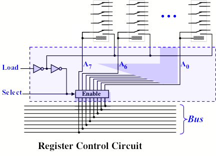
We can simplify the diagram of a register, as follows.
This computer has a number of registers connected to a single bus. Next we show two registers connected to the same bus.
The Address Bus
In addition to the 8-bit data bus, this computer also contains a 16-bit bus, called the “address bus”.
Each of the registers contains 8 bits. However, two registers can be combined to form a single 16-bit register. Whenever two 8-bit registers are combined into 16-bits, the value can be selected or loaded onto the 16-bit address bus.
To achieve this, we duplicate the LOAD/SELECT control circuitry, once for the 8-bit data bus and once for the 16-bit address bus.
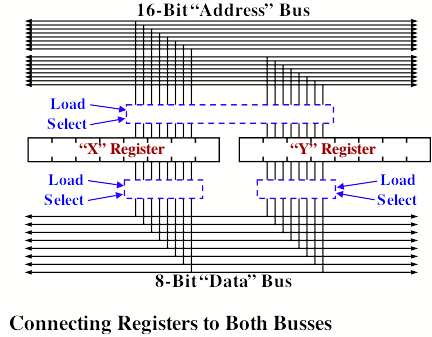
As an example, the computer contains two registers, named “X” and “Y”, which can be combined into a 16-bit register, which is called “XY”. Some instructions deal with the 8-bit registers, including X and Y, and these instructions use the data bus. There are other instructions that deal with 16-bit registers, like XY, and these instructions use the address bus.
Overall System Architecture
The next diagram shows the complete system architecture.
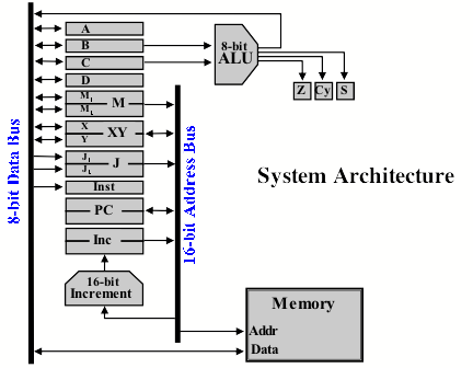
The 8-bit data bus is shown as a single heavy line, although there are of course 8 parallel wires. Likewise, the address bus is shown as a single line, instead of showing all 16 wires.
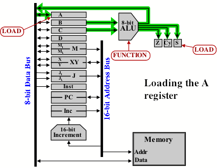
Each register is characterized as a rectangle. The “general purpose” registers are all 8 bits. They are:
A
B
C
D
M1
M2
X
Y
Each of the general purpose registers can be LOADed or SELECTed onto the data bus, as indicated with the double-ended arrows.
The X and Y registers can be combined into a 16-bit register, called “XY:”. The 16-bit value can be SELECTed or LOADed from the address bus.
The M1 and M2 registers can be combined into a 16-bit register, called “M”. The 16-bit value can be placed on the address bus, however, the combined 16-bit register cannot be loaded from the address bus. This is indicated by the direction of the arrow, which shows that M can be SELECTed but not LOADed from the address bus.
In addition, there are several other registers, which have specific uses.
The J register is a 16-bit register used during BRANCH and CALL instructions. It is loaded byte-by-byte, and so is divided into registers called J1 and J2, each 8 bits in width. These are LOADed from the data bus.
The INST register is 8 bits. During instruction execution, INST contains the current instruction being executed. The INST is only loaded from the data bus. Its value is used by the control circuitry (not shown here) and its value cannot be SELECTed onto either bus.
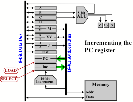
The PC (i.e., Program Counter) is a 16-bit register. The PC contains the address of the next instruction to be executed. In some computers, this register is called the “Instruction Pointer”.
The INC register is a 16-bit register which is used in conjunction with a 16-bit increment unit.
The 16-bit increment unit consists of 16 half-adders circuits. It takes, as input a 16-bit value and produces, as output, a 16-bit result, which is its input, plus one. The 16-bit increment unit takes its input from the address bus. Thus, it is always adding one to the value on the address bus; whenever the address bus changes, the output of the 16-bit increment changes.
The INC register takes as its input, the output of the 16-bit increment unit. When the LOAD control line to the INC register is asserted, the INC register will be loaded with the address bus’s value, plus one.
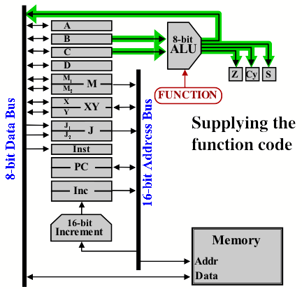
Also shown is the ALU. The ALU takes, as input, the current values in the B and C registers. The ALU also takes 3 control inputs, but this diagram does not show control lines. The ALU produces an 8 bit result which is connected directly to the data bus. Whatever value the ALU is producing is placed on the data bus. Normally, the ALU control input is 111, the <not used> function code, so the ALU is effectively disconnected from the data bus.
The ALU also produces three additional bits of output:
Z – Zero
Cy – Carry Out
S – Sign
There is a 3-bit register called the “Condition Code Register”, which is shown in this diagram. When the condition code register is loaded, the 3 bits are set to reflect the Zero/Carry/Sign of the ALU result. The value stored in the condition code register is used by the control circuitry, in particular, by the CONDITIONAL BRANCH instructions.
Finally, the diagram shows the computer’s main memory. The memory takes, as an address, the 16-bit value on the address bus. During a memory LOAD operation, data is moved from the memory onto the data bus, and then into one of the registers. During a memory STORE operation, data is moved from a register, onto the data bus, and into the memory.
Physical Organization of Major Functional Units
The computer is housed in four cabinets (called “units”) and each is meant to be positioned in the following order.
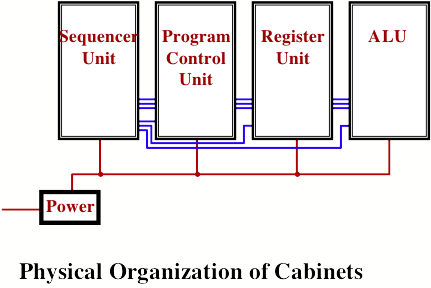
The cabinets are normally hung on the wall, but they have rubber feet and can be placed side-by-side on a table. The power supply is meant to sit on the floor, out of the way.
There are a number of connections between the four cabinets. For example, the 8 bit data bus is routed all the way through from the Sequencer Unit to the ALU, since all units contain connections to the data bus. There are also control line connections from the Sequencer Unit to the each of the three other units.
All the cables between the cabinets use connectors so that the cabinets can be disconnected from one another and moved independently.
The Arithmetic Logic Unit
The rightmost cabinet houses the Arithmetic Logic Unit (ALU). It has the following external connections:
B Input (8 lines)
C Input (8 lines)
Result / Data Bus (8 lines)
Function Code (3 lines)
Condition Code Outputs: Z, Cy, S (3 lines)
Power and Ground (2 lines)
The ALU contains a row of 8 LEDs and 8 switches for the B input and another row of 8 LEDs and 8 switches for the C input. If connected to the register unit, the ALU takes its input from the B and C registers. If not connected, the B and C inputs can be entered directly using the switches.
The ALU also contains a row of 3 LEDs and 3 switches for the function code. If connected to the Sequencer Unit, the function is controlled by the Sequencer Unit. If not connected, the function code can be entered directly.
The importance of being able to enter the function code and the B and C inputs directly using switches is that the ALU can be thoroughly and efficiently tested independently of the other units.
The ALU also contains a row of 8 LEDs for the result. In addition, the ALU contains a row of LEDs for each of the partial results:
Output of the 8-bit adder
AND
OR
XOR
NOT
SHL
The LEDs of the partial results will change whenever the B or C inputs change, even though the partial results may not be enabled onto the result bus.
There are also LEDs for the CARRY and ZERO outputs. (There is no LED for the SIGN, since it is nothing more than the most significant bit of the result.)
The Register Unit
One of the four cabinets in the computer is called the “Register Unit”. It contains the eight general purpose registers: A, B, C, D, M1, M2, X, and Y.
Each of the eight registers was constructed as a separate module. In addition to the relays, each register module contains eight LEDs, which monitor the state of the bit relays in the register. Thus, you can see clearly what value is stored in each register. To the right of each register module are the LOAD and SELECT switches for that register.
Each control line has an associated switch. The switch allows you to manually manipulate the control line. Each switch is connected between power and the control line. In the “OFF” position, the control line is not connected to power; in the “ON” position, the switch connects the control line directly to power. The switches are toggle switches, installed so that they are ON when up, and OFF when down, as you’d expect.
During normal operation, when the computer is running, all switches should be in the down (OFF) position. The control lines are routed back to the sequencer unit and are driven by the state sequencer and control circuitry. However, for purposes of testing and demonstration, the control lines can be manually driven high by the switches.
The Register Unit contains switches for the following control lines, which allows for full control of the registers. In other words, all LOAD and SELECT lines can be manipulated individually.
Ld-A Sel-A
Ld-B Sel-B
Ld-C Sel-C
Ld-D Sel-D
Ld-M1 Sel-M1
Ld-M2 Sel-M2 Sel-M
Ld-X Sel-X
Ld-Y Sel-Y LD-XY Sel-XY
The 8 wires of the data bus are routed more-or-less vertically through the cabinet. At the bottom of the register unit are 8 LEDs and 8 switches which allow the data bus itself to be observed and to be driven directly.
To manually load a value into the D register, for example, take the following actions:
1. Set the 8 data bus switches to reflect the value to be loaded
(0 = switch down; 1 = switch up)
2. Turn the LOAD switch for the D register ON.
3. Turn the LOAD switch OFF.
To manually transfer a value from the D register to the X register, for example, take the following actions:
1. Turn the SELECT switch for the source register (e.g., D) ON.
2. You should see the value from D displayed on the data bus.
(0 = LED is off; 1 = LED is on)
3. Turn the LOAD switch for the target register (e.g., X) ON.
4. Turn the LOAD switch for the target register back OFF.
5. Turn the SELECT switch for the source register back OFF.
The 16-wires of the address bus are also routed more-or-less vertically through the register unit. You can, for example, load a 16-bit value into M (by loading M1 and then loading M2). Then you can select all 16-bits of the combined M register and, using the address bus, LOAD the XY register in one step.
Since the address bus is used, instead of the data bus, the data bus LEDs will not come on during a 16-bit move. In fact, the data bus can be used simultaneously to move 8-bits between two other registers while M is moved into XY.
The Register Unit has the following external connections:
Data Bus (8 lines)
Address But (16 lines)
Control Lines (19 lines)
B Register (8 lines, to ALU B input)
C Register (8 lines, to ALU C input)
Power and Ground (2 wires)
The four units of the computer are meant to be placed in side-by-side in a particular order, so some of the connections above are duplicated. For example, the 8 lines of the data bus come into the left side of the cabinet, from the Program Control Unit, and go out the right side of the cabinet, on to the Arithmetic Logic Unit.
The Program Control Unit
The Program Control Unit contains the following modules:
J1
J2
INST
PC-1
PC-2
INC-1
INC-2
16-bit Increment Unit
For ease of construction, the PC and INC registers were each broken into two 8-bit register modules, even though they are only used as 16-bit registers.
The Program Control Unit contains switches for the following control lines.
Ld-J1
Ld-J2
Sel-J
Ld-Inst
Ld-PC
Sel-PC
Ld-INC
Sel-INC
The 8 wires of the data bus and the 16-wires of the address bus are routed more-or-less vertically through the cabinet.
There are 16 LEDs and 16 switches for the address bus at the bottom of the Program Control Unit.
The Program Control Unit has the following external connections to the Sequencer Unit to the left:
Data Bus (8 lines)
Address But (16 lines)
Control Lines (8 lines)
Inst Register (8 lines, to the Sequencer Unit)
Power and Ground (2 wires)
In addition, the Data Bus, the Address Bus, and the Power and Ground lines are also connected to the Register Unit to the right.
Main Memory
The main memory is implemented with a 32K byte static RAM chip, which is located in the lower left corner of the Sequencer unit.
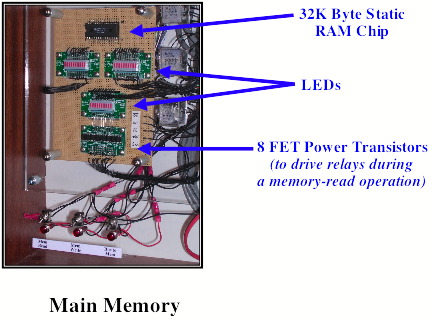
In order to address 32K bytes, only 15-bits are needed. The memory sub-circuit ignores the most significant bit of the address bus.
An Example of Instruction Execution
In the next series of figures, we show the steps involved in the execution of an instruction. As an example, we’ll show each step in the execution of an “ADD” instruction. This is one of the “ALU instructions” (ADD, INC, AND, OR, XOR, NOT, and SHL) which are all quite similar. The ALU instructions take their inputs from registers B and C and place their result in register A. All ALU instructions are executed identically, and differ only in the operation (ADD, INC, etc.) actually performed.
In the first step, the Sel-PC (“select PC register”) control line goes high, which causes the program counter to be gated onto the 16-bit address bus. In the next few diagrams, the control lines are shown with red arrows to indicate that they are asserted, i.e., driven high. The green arrows show data flow on and off the buses.
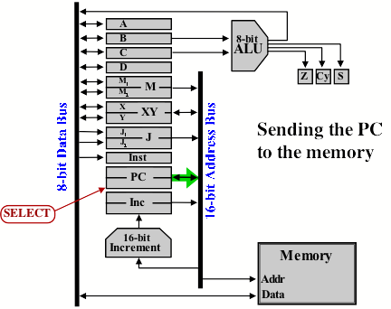
At the same time, the Mem-Read control line goes high. This gates the output of the static RAM onto the 8-bit data bus.
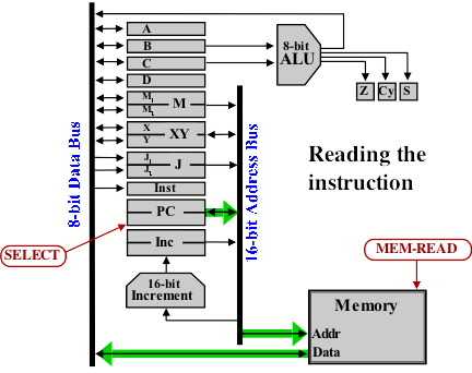
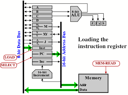
In the next step, the Load-Inst control line goes high, which causes the 8 bit instruction register to be loaded.
The Program Counter is always incremented at the beginning of each instruction. This takes two steps: first the “Inc Register” is loaded with the old value of the PC, plus one; then the new value is copied from the Inc Register back to the PC register. The first step can be overlapped with the fetching of the instruction from memory.
The Increment Unit is always taking whatever value is on the address bus and adding 1 to it. The incremented value is directed toward the “Inc Register”. So the first step is simply to load the Inc Register with this value.

The second part of incrementing the PC is to copy the new value from the Inc register back to the PC. First the Inc register is gated onto the address bus. Then the Load-PC control line is asserted to load the PC register.
The above steps are done at the beginning of each instruction. Only at this point, after the Inst register is loaded, do we know what instruction is being executed. Only after this point can we take action that is different from instruction to instruction.
All ALU instructions contain a 3-bit field containing the function code, which tells whether the instruction is an ADD, INC, etc. In the next step, after seeing that this is a ALU instruction, the function code is gated from the instruction register to the ALU Function Code control lines.
The 8-bit result of the ALU will only be gated onto the data bus when a valid function code is supplied. For all other instructions, the control unit will supply the <NOT USED> function code to the ALU.
The computer also contains a 3 bit register containing the condition codes. There is a bit for ZERO, CARRY, and SIGN. The ALU produces these 3-bits, which are routed to the Condition Code register.
In the final step, the control unit asserts the Load-A control line and the Load-Cond control line. This loads the A register with the result from the ALU, via the data bus and loads the 3-bit condition code register with appropriate values from the ALU.
The Clock Circuit
Before we can discuss how the control unit operates and how it sends out the
control signals, we need to discuss the clock circuitry. The “Clock Circuit” has, as its goal,
providing a single steady square wave to the rest of the computer. This is essentially the heartbeat of
the computer, which regulates the speed and timing of the control signals.
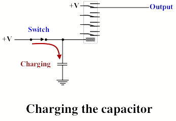
The clock circuit uses capacitors and we will develop it in stages.
A capacitor is a little like a battery: when connected to power it is charged up. When unconnected from the power, it is capable of providing power for a short time to drive some other load.
Consider the following circuit, which contains a relay, a switch, and a
capacitor.
When the switch is closed, the capacitor will be charged up. In addition, the relay will be turned on and the output will go high.
If the switch is then opened, the capacitor will begin discharging. Notice that the relay will stay on because the capacitor is providing power to the relay. Thus, even after the switch is opened, the output will stay high.
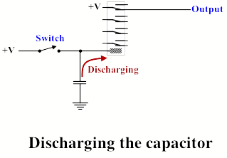
In a short time, the capacitor’s charge will be depleted and the relay will finally turn off. The output will then go low.
The capacitor is introducing a small delay. When the switch is closed, the output goes high. When the switch is opened, the output will go low, after a short delay. The length of the delay is determined by the size (i.e., the rating) of the capacitor.
In this computer, a value of 0.5 farad (which is quite large, for a capacitor) will keep the relay on for approx 1/5 second.
Some readers familiar with electronic circuits will note that this circuit involves a capacitor and a coil connected together. These readers may spot an “LC” oscillator circuit here. However this circuit does not operate like a conventional LC circuit. While superficially similar, this circuit will not operate as an effective LC oscillator because the coil involved is a bit different than in an LC circuit. In an LC oscillator, the idea is that the coil stores energy during part of the cycle. The coils used in such circuits are presumably designed to optimize their ability to store energy. On the other hand, the coil in a relay is designed with exactly the opposite goal: the relay coil is designed to emit at much energy as possible, in order to move the switches. While relay coils do have some inductance, this effect has been completely ignored in this computer’s design.
Next consider the following circuit, which is a chain of relays, each wired identically. Each relay has its own capacitor.
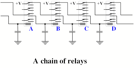
To understand the circuit, assume that relays “A” and “B” happen to be on initially.
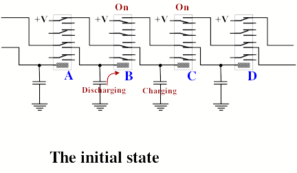
The coil of relay “B” is not connected to power, so the only way it could be on is for its capacitor to be discharging. Meanwhile, the coil of relay “C” is connected to power, so that it will be on and its capacitor will be charging.
After a short time, relay B’s capacitor will finish discharging and relay B will then turn off. This results in the next state:
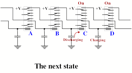
When B turns off, this will disconnect relay C from power. However, C’s capacitor will take over and keep C turned on while it discharges. Also, relay D is now connected to power. Note that relay D has come on and its relay has begun charging.
In the next figure, we have connected relay D back to relay A in the same way, creating a cyclic chain.
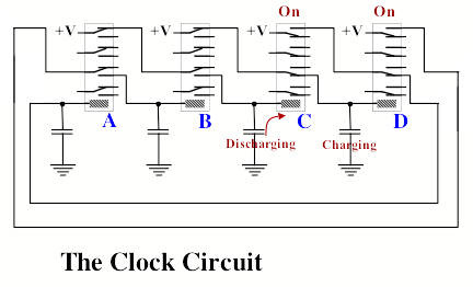
Once started, this circuit will keep clicking away forever in a regular pulsing beat.
One way to understand this circuit is to look at a timing diagram, which shows the values of certain signals over time. In the following timing diagram, we look at the 4 relays in the clock circuit, showing when each turns on and when each turns off.
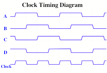
Note that each relay stays on for 2 units of time. During the first time interval, power is supplied to it and its capacitor is charging. During the second interval, power has been cut (by the transition of the relay directly above it) and it stays on while its capacitor discharges.
To get the desired square wave from this circuit, note that the logical formula
Clock = (A and D) or (B and C)
results in the wave shown at the bottom, labeled “clock”.
In the clock circuit, as shown, we only used 2 of the 4 switches in each relay. The “Clock” signal can be created using the remaining switches. Also note that the Clock signal can also be derived with the following formula using “exclusive-or”, which is slightly easier to wire:
Clock = C xor D
The circuit, as described so far, is still not good enough. Recall that I said “once started, this circuit will keep clicking away...” We need to ensure that when the power is turned on, the clock circuit will start up on its own.
We’d also like to be able to “single step” the computer. In other words, we’d like to be able to disable the clock circuit and generate the clock signal manually by flipping a switch up and down. By controlling the clock transitions manually, we can walk the computer through interesting operations at a speed that allows us to observe the computer’s operation. The frequency of the pulse generated by the clock circuit is much too fast to follow.
In addition, we need to be able to freeze the clock, i.e., make it stop ticking. It turns out that this is very useful when operating the computer. You can run it continuously up to some point of interest and then single step it. The idea is that while the clock circuit is generating regular pulses, the human can, at any time, flip a switch to freeze the clock. From then on, the human can flip another switch to perform the single-stepping.
The problem is that the freeze switch can be thrown at any time. In particular it could be thrown just after the Clock signal went high. If the Clock signal doesn’t stay high for a full unit of time, then the last operation may be incompletely performed and the computer may be left in an inconsistent or unpredictable state. This would be unacceptable.
To control the clock circuit, there are three switches, which are labeled:
Oscillator Power
Run / Stop
Single Step
In addition, there is a single light, labeled “Clock”, which monitors the output of the entire circuit to the rest of the computer. It is this signal which drives the Finite State Machine, which will be described later in this document.
Normally, the Oscillator Power is turned on at all times. The Run/Stop switch should be positioned in the Stop position when the computer is powered on. The Single-Step switch should be down.
After loading some registers, the computer can be started by moving the Run/Stop switch to the Run position. Instruction execution will commence and relays will begin clicking. At any point, the switch may be moved back to the Stop position. Then, the Single Step switch may be toggled up and down, up and down, as many times as necessary to slowly walk the computer through instruction execution.
A final design consideration is the HALT instruction. When this instruction is executed, the computer must stop executing instructions. This should be accomplished by freezing the clock circuit, as if the Run / Stop switch were moved into the Stop position.
Next, let’s turn to the problem of making sure the clock begins when the power is initially turned on.
Looking back at the clock circuit, we see that power will be supplied to relay D when B is off and C is on. Something similar is true of all other relays and we can express it like this:
A = ~C and D
B = ~D and A
C = ~A and B
D = ~B and C
If any one relay could somehow be turned on, then some other relay would be switched on and the circuit would being operating. Unfortunately, when the power is turned on, all relays will be off. If we can just get one relay to come on, the cycle will begin.
The secret is to alter the formula for relay A. Relay A must have its power supplied at exactly the same time as before, but we want to achieve this in a different way. Looking at the timing diagram, the idea is to detect the time interval during which power should be supplied to relay A. As designed previously, power is supplied to relay whenever C is off and D is on; this happens exactly when power should be supplied to relay A.
Instead of relay A depending on D being on (which is a problem), the modification is to make relay A depend on B being off. In other words, we will alter the equation for A to:
A = ~C and ~B
This will still supply power to A at the same times as before, but in addition, it will also turn relay A on when the power is initially applied and all relays are off.
In this computer, the clock circuit has a power supply that is switched. In other words, there is a switch (labeled “Oscillator Power”) which provides power to the entire clock circuit. This switch allows the power to the circuit to be cut. Normally, this switch is always left on and the switch labeled “Run / Stop” is used to freeze the clock circuit for single stepping.
The Run/Stop switch works as follows: When the switch is moved into the Stop position, power is supplied to a line called “freeze”. (The Run/Stop switch happens to be mounted in the opposite orientation from all the other switches, since the closed position (“Stop”) is with the lever down, instead of up.)
Notice that if relay A were to come on and then, for some reason, stay on even after its capacitor fully discharged, relay B would continue to stay on and relay C would never come on. The clock circuit would freeze, and it would freeze in a state in which the output (the “Clock” line) was low.
So by using another switch in relay A, we can arrange that whenever it comes on, it will latch on and stay on, whenever the Freeze line is high. This is just a simple latch circuit like we saw with the registers, in which power is routed to the coil of a relay through one of the switches in the relay. Once on, the relay stays on. The only difference here is that instead of using unswitched power to keep the relay on, we use the Freeze line. When Freeze is high and the relay turns on, it will stick and stay on. When Freeze is low, it will have no effect and the clock circuit will continue to cycle as before.
Likewise, we can arrange that relay C will latch and stay on, whenever the Freeze line is high.
The benefit of this approach to implement freezing by latching relays A and C is that the computer will not freeze the instant the Run/Stop switch is moved to Stop. Instead, the clock circuit will continue until it gets to a state where the Clock output is low. Only then will the relays stop changing and the Clock output will remain low forever.
Consider what happens when the Run/Stop switch is moved to Stop when the clock is high (for example, while relays A and D are on). Since the Freeze line is now high, relay A will latch and stay on. Relay D’s capacitor will continue to discharge until D turns off. The Clock output will then go low and relay B will turn on. Nothing further will happen.
The Single Step switch works by simply driving the Clock output line high directly. The normal procedure is to first freeze the clock circuit by turning the Run/Stop switch to Stop and then manually operating the Single Step switch.
The last problem to be addressed by the clock circuit is the handling of the HALT instruction.
When the HALT instruction is executed, it will turn on a relay which will latch on and stay on. This relay is called the “Halt Relay” and is numbered R40. When on, the Halt relay will also cause the Freeze line to be asserted. Once on, this clock circuit will freeze, as just described.
The Halt relay is latched using the switched power to the clock circuit. Once it turns on, the Halt relay will stay on until the switch labeled “Oscillator Power” is cycled. The single step switch also goes through the Halt relay so that single stepping cannot be done after the HALT instruction is executed.
In this computer, the Clock line changes 5.6 times per second (i.e., every .17708 seconds). I prefer not to say "cycles per second" (which would be 2.8 cps), because some actions happen on clock-up and others on clock-down. The instructions take between 8 and 24 clock transitions (i.e., between 1.4 seconds and 4.25 seconds).
The Finite State Machine
A finite state machine has number of “states” which are connected with “transition edges”. Sometimes they are called “finite state automata” and we’ll use the abbreviation “FSA”. The following FSA has 8 states, connected in a simple cycle. In this example, there are no choices about which state to go to next, but we’ll see a more complex FSA soon.
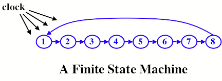
At any one time, the FSA is in one of the states and, as time goes on, the FSA moves from one state to the next. In this computer, the FSA circuit is driven by the output of the Clock Circuit. Each tick causes the FSA to follow the next edge to the next state. In particular, each clock transition causes the FSA to move from one state to the next.
We can construct a circuit to implement an FSA using a chain of relays, using logic similar to the Clock Circuit.
The next step is to pull timing signals off the FSA. For each state, there is a corresponding output line. When the FSA is in a state, such as the state labeled “3”, we get a pulse along the corresponding line. This line remains high as long as the FSA is in state 3.
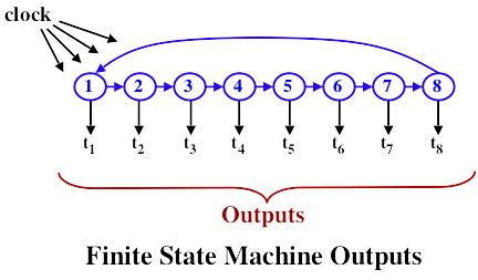
Let’s label the outputs from the FSA with names t1, t2, t3, etc.
In the timing diagram shown next, we can see that each timing line stays high for a complete clock tick and that these lines are activated in a repeating cycle.
These timing signals are used to sequence the computer through the execution of an instruction. Many instructions, such as the ADD instruction, take 8 time units. (Other instructions take more time units to complete, but we’ll deal with this complication later.) Each time the FSA makes one cycle through all its states, a single instruction is executed.
The Timing of an Instruction
Next, let’s look at the execution of the ADD instruction. In particular, we’ll look at the following control lines:
Select PC
Memory Read
Load Instr
Load Inc
Select Inc
Load PC
ALU Function (f0, f1, f2)
Load A Reg
Load Cond. Code Reg
These control lines will need to go high during some portion of the execution of the ADD instruction. The other control lines will not be needed and will remain low during this instruction.
[Warning: In this paper, the naming of the control lines is not consistent. For example, the “Select PC” line is also called “Sel-PC”.]
Here is a diagram showing the exact sequencing of the control lines to achieve the execution of the ADD instruction.
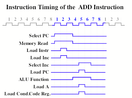
Each of these control lines has a switch on the front panel of the computer. Thus, you could manually execute the actions of an ADD instruction by flipping these control lines in exactly the order shown in this diagram.
[Note: If you want to do this, you’ll need to make sure the FSA and associated control circuitry is not active. This can be done by turning off the switches labeled “Oscillator Power” and “FSA Power.” You may also want to go through the steps to load the B and C registers with some values to be added, before you start.]
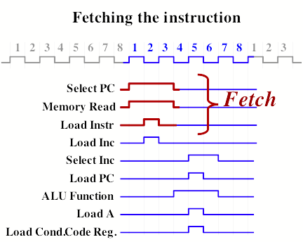
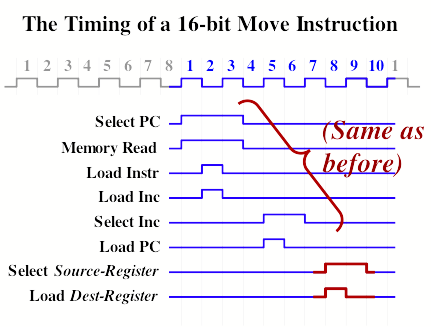
Next, let’s look at this timing diagram in more detail. The basic model of instruction execution in any computer involves the so-called “fetch-increment-execute” loop, which means that the execution of every instruction involves these three steps. The first is to fetch the instruction from memory; the second is to increment the Program Counter so that the next instruction will be fetched from the next sequential location; and finally to execute the instruction.
The “fetch” and the “increment” operations are the same for every instruction. The “execute” portion is different for each kind of instruction and exactly what happens will be determined by the nature of the instruction actually retrieved from memory during the “fetch”.
The next diagram highlights in red the “fetch” portion of the instruction. We can see that we are gating the PC onto the address bus (Select PC) and are asking the memory to read a byte and place it on the data bus (Memory Read). Then the Load Instr control line is asserted to load the 8-bit instruction register from the data bus.
In the next timing diagram, the control signals associated with incrementing the PC are highlighted in red.
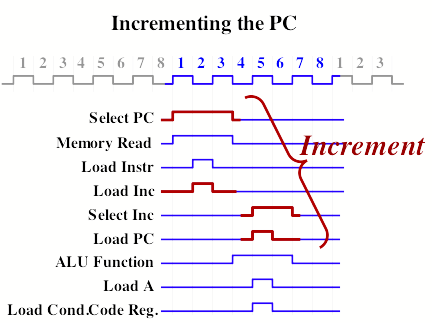
In the first step, we are gating the PC onto the address bus (Select PC) and loading the Increment Register (Load Inc). The Increment Register is loaded with the value on the bus, plus one. In the second step, we are gating the Increment Register onto the address bus (Select Inc) and loading the PC (Load PC).
Note that the fetching and incrementing overlap in time. The PC is put onto the address bus and used by two things at once: the memory and the increment circuitry.
All instructions begin with this same sequence of timing signals. After the instruction register has been loaded, however, the control signals particular to the individual instruction can begin.
In the next diagram, we show the control signals associated with any ALU instruction. In our example, we are looking at an ADD instruction, but the INC, AND, OR, XOR, NOT, and SHL instructions have the same control signals and differ only in the particular function code.
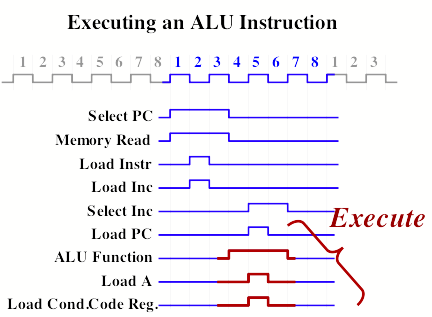
The B and C registers are always supplied to the ALU, so the ALU only needs the 3-bit function code, telling which operation is selected, to output the correct result onto the data bus.
The ALU instructions all have the following bit pattern:
1 0 0 0 R F F F
The first 4 bits indicate that this is an ALU instruction. The 3 bits marked FFF contain the 3-bit function code and determine which operation is required. (The function code for ADD is 000, the function code for INC is 001, etc.) The ALU can load its result into either the A register or the D register; the bit marked R determines which register will be loaded.
For example, to add B and C and put the result in A, the instruction op-code would be:
1 0 0 0 0 0 0 0
As the timing diagram shows, the function code is supplied to the ALU during time periods 4, 5, and 6. During time period 5, if the “R” bit is 0 then the Load-A control line is asserted. However, if the “R” bit is 1 then the Load-D control line is asserted.
The ALU operations also save the condition codes, so in period 5, the control line called “Load Cond. Code Reg.” is asserted. This will save the status of the “zero”, “carry”, and “sign” bits associated with the operation performed by the ALU.
The “Condition Code Register” is located in the Sequencer Unit near the relays marked “Instruction Decoding”. This register is somewhat unusual since it is not “on” any bus. Instead, it takes its input from only one source (the ALU) and is used only during the execution of conditional branch instructions. For example, after an ADD instruction, the program may contain an instruction to test whether the result was zero, i.e., to branch if and only if the “zero” bit in the condition code register is set.
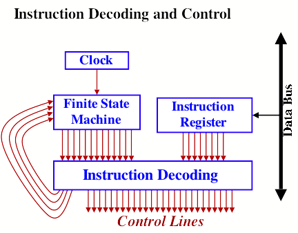
Instruction Decoding
The next thing to understand is how control signals, such as those shown for the ADD instruction, are generated. This is the task of the module labeled “Instruction Decoding”.
We’ve seen how the finite state machine (the FSA) provides signals telling which period of time it is currently. For example, the control line to load the PC must go high during time period 5, i.e., when the line called “t5” is high. The outputs from the FSA provide inputs to the Instruction Decoder.
Also, after time period t3, the Instruction Register has been loaded. After this point, the execution of the instruction can depend on which instruction is being executed. Therefore, the Instruction Register also provides inputs to the Instruction Decoder, with the proviso that the Instruction Register must not used as input before time t3.
The outputs of the Instruction Decoder are simply the control lines. There are 34 outputs from the Instruction Decoder.
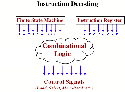
Connecting the inputs to the outputs, we have some “combinational logic”. Combinational logic is functional, in the sense that the outputs depend only on the inputs. There is no state. Any combinational logic can be constructed using simple logic gates such as AND, OR, and NOT and we know even how to design and optimize combinational circuitry automatically.
One place where care must be taken is with transitions. Consider the Select-PC control line, which must be high during time t1, t2, and t3. You might be tempted to derive the Select-PC with this equation:
Select-PC = t1 OR t2 OR t3 OR <other terms>
The Select-PC line will needed to be asserted in other times, for example during branch instructions, and the <other terms> allude to this.
The problem is that the select-PC line must stay high continuously during t1, t2, and t3. We must guarantee that the output from the FSA will not go low momentarily between say t1 and t2. If so, we might have a “glitch”, which could affect the correct operation of the computer.

Glitches can also happen in the opposite direction, in which a line goes high
for a short time, when it should stay low. If a control line erroneously goes high for long enough, it
would be a disaster, perhaps causing a random register to be loaded
incorrectly.
Glitches like this can occur in combinational logic, if not carefully designed. In combinational logic, you are traditionally guaranteed that the output will be correct some time after the inputs have stabilized. (This is the delay of the circuit which, in electronic designs, we often want to minimize.) What can happen is that, when an input changes, the output can go through some incorrect outputs before it settles on the correct output.
In modern electronic circuit design, unlike this relay computer, all registers are loaded on the leading, rising edge of a clock signal, while their outputs become valid on the trailing, falling edge. The circuit’s combinational logic works between then falling clock edge and the next rising clock edge. Any glitches that occur are ignored, since the output of the combinational circuits is not used until the next rising clock edge.
My solution to the problem of glitches is to create a intermediate set of “timing signals”. There are 19 timing signals. The FSA outputs the timing signals and they are supplied as input to the combinational logic of the Instruction Decoding.
The timing signals are like the FSA outputs t1, t2, t3, etc., except that some of them last 2 or 3 time periods, instead of just one period. However, many of the timing signals last only one period and are, in fact, nothing more than the outputs of the FSA.
Longer Instructions
As mentioned above, some instructions take more than 8 clock periods. For example, one instruction can move data from one 16-bit register to another. Since this instruction uses the address bus to move the data, it cannot perform its “execute” phase until the address bus is free.
This instruction takes 10 clock periods. Actually, it could be done in 9 periods, but due to the nature of the up-down cylce of the Clock Circuit, all instructions take an even number of clock periods.
The longest instruction takes 24 clock periods to execute. Other instructions take 8, 10, 12, and 14 clock periods. So here is the complete finite state machine, with 24 states.
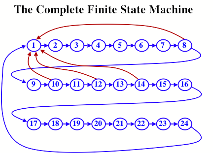
We can view the FSA as a machine that cycles from state 1 to state 24, with the exception that some instructions are “aborted” earlier, sending the FSA back to state 1 prematurely. Perhaps “abort” is not the best term, since there should be no negative connotation for an instruction that executes in only 8 or 10 clock periods.
To implement this, we must modify the FSA to make conditional transitions after states 8, 10, 12, and 14. Now, the FSA gets a little more complex, taking inputs from the combinational logic.
The Sequencer Unit contains the Clock Circuit at the top. Below that is the module labeled “Finite State Control” which is the FSA. There is an LED for each of its 24 states and as instruction execution occurs, the state lights illuminate in sequence. By watching these, you can see when each instruction begin execution. You can also see which instructions last only 8 states and which go all the way to state 24.
Below the FSA is a row of 19 LEDs, with one for each of the 19 timing signals. To the right of that is a row of 8 switches and LEDs for the instruction register. The 8 LEDs show the instruction being executed and the switches allow an instruction to be entered directly, which was useful during testing of the combinational Instruction Decoding logic.
Both the timing signals and the Instruction Register form the inputs to the Instruction Decoding logic, which lies just below. Below the Instruction Decoding, you’ll see 34 LEDs, one for each control line. Thus, the inputs to the Instruction Decoding are above it, and the outputs are below it.
Each of these 34 LEDs is connected to the corresponding control line and is routed to other parts of the computer. For example, one output of the Instruction Decoding is Select-PC. Thus, there is an LED with that label, which will go high during t1, t2, and t3 of each instruction’s execution.
There are also 8 LEDs below the Instruction Decoding showing the instruction class, which is derived as part of the Instruction Decoding logic. These LEDs are labeled with the following instruction classes:
MOV-8
SETAB
ALU
LOAD
STORE
MOV-16
INC-XY
GOTO
The Instruction Set
Each instruction is one byte long. Furthermore, several instructions also include two additional bytes, making these instructions three bytes in total. The second and third bytes form a 16-bit value, which is usually used as a memory address.
In the next few sections, we discuss each individual instruction.
The 3 bits of the condition code register (Zero, Carry, Sign) are modified by only the ALU instruction.
MOV-8: The 8-Bit Move Instruction
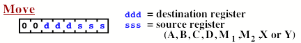
This instruction moves the contents of one of the 8-bit registers to any other register.
If the “source” and “destination” register happen to be the same, this instruction will set that register to zero. In many computers, this function is called the “CLEAR” instruction.
Register Codes (ddd and sss):
000 = A
001 = B
010 = C
011 = D
100 = M1
101 = M2
110 = X
111 = Y
This instruction takes 8 clock periods.
ALU: The ALU Instructions
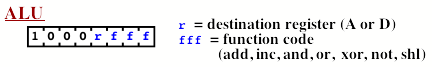
This instruction takes, as its input, the current values of the B register and the C register. The result is placed in either the A register or the D register. A single bit in the instruction (called “r”) indicates whether to put the result in A or D. The function to be performed is encoded in the 3-bits called “fff”.
Destination Register Code (r)
0 = A
1 = D
Function Codes (fff)
000 = ADD
001 = INC (increment B by 1)
010 = AND
011 = OR
100 = XOR
101 = NOT
110 = SHL (shift B left circular 1 bit)
111 = <not used>
The INC, NOT, and SHL functions use only B and ignore C. If the function code fff is 111 (i.e., <not used>), then zero will be loaded into the destination register. All 3 bits of the condition code register (Zero, Carry, and Sign) will always be updated, regardless of what function code is used.
This instruction takes 8 clock periods.
SETAB: The Load Immediate Instruction
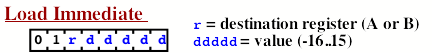
This instruction can load any value between –16 and +15 into either the A register or the B register.
Destination Register Code (r)
0 = A
1 = B
The 5-bit value (ddddd) is first sign-extended to 8 bits, which allows negative numbers to be specified.
This instruction takes 8 clock periods.
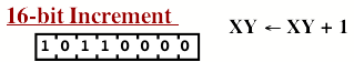
INC-XY: The 16-Bit Increment Instruction
This instruction increments the XY register.
This instruction takes 14 clock periods.
LOAD: The Load Instruction
![]()
This instruction reads a byte from the SRAM memory and moves it into one of 4 possible registers. The memory address is taken from the 16-bit M Register.
Destination Register Code (rr)
00 = A
01 = B
10 = C
11 = D
This instruction takes 12 clock periods.
STORE: The Store Instruction
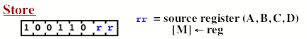
This instruction writes a byte from one of 4 possible registers into the SRAM memory. The memory address is taken from the 16-bit M Register.
Source Register Code (rr)
00 = A
01 = B
10 = C
11 = D
This instruction takes 12 clock periods.
MOV-16: The 16-Bit Move Instruction – General Form
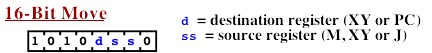
Destination Register Code (d)
0 = XY
1 = PC
Source Register Code (ss)
00 = M
01 = XY
10 = J
11 = zero <and halt>
This instruction copies 16 bits from one register to another. Either the XY register or the Program Counter (PC) may be loaded. If the PC is selected as the destination, this will cause a branch in program execution.
If the source register code is 11, then the value zero will be moved and furthermore, instruction execution will be suspended.
The CALL instruction (discussed below) will branch and save the return address in XY. Thus, by moving XY back to the PC, this instruction can be used as a RETURN instruction.
This instruction takes 12 clock periods.
MOV-16: The Halt Instruction
This instruction is a special case of the more general 16-bit move instruction.
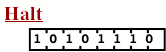
Execution will halt at the completion of this instruction. Furthermore, the PC will be loaded with zero, which is often handy if you want to rerun the program from the beginning (and the program starts at location zero).
MOV-16: The Return / Branch-Indirect Instruction
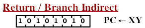
This instruction is a special case of the more general 16-bit move instruction.
This instruction will copy the 16-bit value in the XY register to the Program Counter (PC), which will cause a branch (i.e., a “jump”) immediately thereafter.
The CALL instruction (which is discussed below) will jump to a subroutine and will also save the “return address” in the XY register. The subroutine, after completing execution, can return by moving the address in XY back into the PC with this instruction.
[Most computers save return addresses on some sort of stack, which permits subroutines to call other subroutines, and even to call themselves recursively. This computer does not directly support a stack. Instead, this computer uses a simpler approach of saving the return address in a register. This approach supports subroutines—an important programming abstraction—as long as they don’t call other subroutines. If you wish to call one subroutine within another subroutine, then your program will need to save the return address before calling the second subroutine. A simple STORE and LOAD will suffice if the subroutine is not recursive. By the way, the MIPS microprocessor also uses this approach because of its efficiency; many subroutines don’t call other subroutines and would be slowed down by having to access memory.]
This form of the 16-bit move instruction can also be used to branch to an arbitrary computed memory address. This would be useful, for example, in implementing jump tables, switch statements, or threaded execution models.
GOTO: The Goto Instruction – General Form
The final instruction class is rather unusual and encompasses several different instruction variants. In the sections following this one, we’ll show specific useful examples.
![]()
Instruction Codes
d: destination (0=M, 1=J)
s: 1=load PC if “sign” bit is set (if negative); 0=ignore sign bit.
c: 1=load PC if “carry” bit is clear (if no carry); 0=ignore carry bit.
z: 1=load PC if “zero” bit is set (if result is zero); 0=ignore if “zero” bit is clear.
n: 1=load PC if “zero” bit is clear (if result is not zero); 0=ignore if “zero” bit is set.
x: 1=copy PC to XY; 0=do not copy.
This instruction is followed by 2 additional bytes, which contain a 16-bit address value. This value will be loaded into either the M register or the J register. If loaded into the J register, this instruction will branch to the given address. This is useful for its “CALL” and “GOTO” variants. Alternately, the M register can be loaded with a literal 16-bit value, which is especially handy if the next instruction is a LOAD or STORE instruction, which use the M register as a memory address.
This instruction takes 24 clock periods. During the execution of the instruction, the PC is incremented 3 times. The first is the increment that is done for every instruction. The second and third increments are done in conjunction with loading the second and third bytes of the instruction. Afterward, the PC will be left pointing to the instruction following the 16-bit address portion of the instruction.
In the last step of the instruction, the PC will be loaded from the J register, and this load can be done either conditionally or unconditionally. Normally, this instruction is used either (1) to load the M register (in which case the PC is not loaded and no branching occurs) or (2) to branch (in which case the J register is loaded and then the PC is loaded from J).
The purpose of the J register is solely to support branching instructions where the 16-bit target address follows the 8-bit instruction op-code. Memory is always read one byte at a time. During instruction execution, the PC is used to provide sequential addresses while fetching the 16-bit target address. This target address is fetched and placed into the 16-bit J register. Only after the address is complete is the target address moved from J into the PC, causing the jump in the flow-of-control. Furthermore, this final modification of the PC is conditional. Thus, this instruction can be used to implement conditional branching.
The instruction is also capable of copying the PC register to the XY register. This is controlled by the “x” bit in the instruction. If the x bit is set, then the PC will be copied to the XY register at the end of the instruction, thereby setting XY to point to the next instruction following this instruction. This is useful in the CALL variant of the instruction, when a subroutine is invoked. The instruction following the CALL is the return address.
Here is a summary of the actions this instruction may take, in the order they are executed:
Instr = (PC++)
M1 or J1 = (PC++)
M2 or J2 = (PC++)
XY = PC
PC = J (this step is conditional)
The following chart shows the common variants of this instruction. The SETM instruction moves 16-bits into the M Register; the GOTO (also called JUMP) instruction branches unconditionally; Bcond represents several instructions which branch conditionally (as discussed below); the CALL instruction is used to save a return address and jump to a subroutine.
SETM GOTO Bcond CALL ACTION
Ö Ö Ö Ö Instr = (PC++)
Ö Ö Ö Ö M1 or J1 = (PC++)
Ö Ö Ö Ö M2 or J2 = (PC++)
Ö XY = PC
Ö ? Ö PC = J
The final load (from J into the PC) is conditional, based on the values of the condition code register and several tests selected by the instruction. There are four possible tests, corresponding to four bits in the instruction. The bits in the instructions are called s, c, z, and n. If a bit in the instruction is set to 1, the corresponding test of the condition codes is done. If the test is true, the PC is loaded. If the test is false, or if the test is not selected (i.e., the bit in the instruction is 0), then the PC is not necessarily loaded. If any of the tests is true, then the PC is loaded and a branch occurs. If all the tests are either false or not done, then the PC is not loaded.
Here are the 4 bits from the instruction and their meanings:
s (Sign)
1: load PC if the “sign” bit is set (i.e., if result of last ALU instruction was negative)
0: do not test the “sign” bit.
c (Carry)
1: load PC if the “carry” bit is clear (i.e., if no carry after an ADD or INC instruction)
0: do not test the “carry” bit.
z (Zero)
1: load PC if the “zero” bit is set (i.e., if result is equal to zero)
0: do not test whether the “zero” bit is set.
n (Not Zero)
1: load PC if the “zero” bit is clear (i.e., if result is not zero)
0: do not test whether the “zero” bit is clear.
For example, if only the “s” bit is set, the branch will occur only if the result is negative. Otherwise, the next sequential instruction will be executed. We call this variant “BNEG”, for “branch if negative”.
Here are some common test combinations:
s c z n
0 0 0 0 Never – Used to load the M register with no branching
0 0 1 1 Always – Used for unconditional branching (i.e., the GOTO instruction)
0 0 1 0 BZ/BE – Branch if result zero; Branch if B==C after XOR instruction
0 0 0 1 BNZ/BNE – Branch if result not zero; Branch if B!=C after XOR instruction
0 1 0 0 BNC – Branch if no carry (useful after ADD or INC)
1 0 0 0 BNEG – Branch if result if negative
GOTO Variant: The SETM Instruction
This instruction is a special case of the more general form of the GOTO instruction.
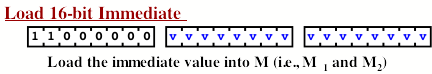
This instruction will load a 16-bit value into the M register (i.e., into the M1-M2 register pair). This instruction is especially useful in conjunction with the LOAD and STORE instructions which expect the M register to contain an address.
GOTO Variant: The JUMP Instruction
This instruction is a special case of the more general form of the GOTO instruction.
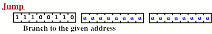
This instruction will branch unconditionally to the address given in the instruction. Sometimes this variant is called the GOTO instruction, but the term “GOTO” is used here to refer to the more general form, which includes other variants.
GOTO Variant: The CALL Instruction
This instruction is a special case of the more general form of the GOTO instruction.
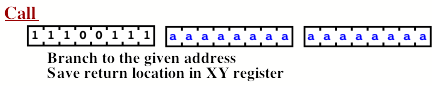
This instruction is used to call a subroutine. It will branch unconditionally to the address given in the instruction. In addition, this instruction will save the address of the next instruction in the XY register. Thus, after completing the subroutine, execution can return to the instruction following the Call instruction.
GOTO Variant: The BNEG (Branch-If-Neg) Instruction
This instruction is a special case of the more general form of the GOTO instruction.
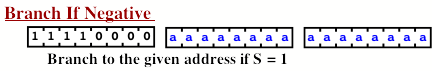
This instruction will branch to the address given in the instruction if the “sign” condition code bit is set to 1. In other words, it will jump if the last ALU instruction (i.e., ADD, INC, AND, OR, XOR, NOT, or SHL) produced a negative result, and not jump otherwise.
GOTO Variant: The BNC (Branch-If-No-Carry) Instruction
This instruction is a special case of the more general form of the GOTO instruction.
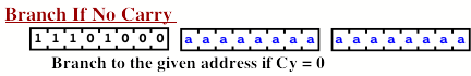
This instruction will branch to the address given in the instruction if the “carry” condition code bit is clear (i.e., zero). In other words, it will jump if the last ADD or INC instruction did not result in a carry, and will not jump if the instruction did carry. [Note that the “carry” bit, like the “sign” and “zero” bits, is modified after every ALU instruction, including AND, OR, XOR, NOT, and SHL. The carry bit will always be set from the 8-bit adder circuit, reflecting whether there would have been a carry if B and C had been added, even if the result selected was not from the 8-bit adder circuit. This is not a nuisance since the programmer would normally test the carry bit only after an ADD or INC instruction.]
GOTO Variant: The BZ (Branch-If-Zero) Instruction
This instruction is a special case of the more general form of the GOTO instruction.
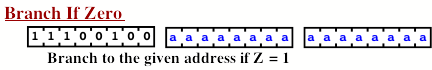
This instruction will branch to the address given in the instruction if the “zero” condition code bit is set to 1. In other words, it will jump if the last ALU instruction (i.e., ADD, INC, AND, OR, XOR, NOT, or SHL) produced a result of zero, and not jump otherwise.
Note that this instruction and the next instruction can be used to test equality. If two values are combined using the XOR instruction, the result will be zero if and only if they are exactly equal. Thus, this instruction is sometimes called the “BE” (i.e., Branch-If-Equal) instruction.
GOTO Variant: The BNZ (Branch-If-Not-Zero) Instruction
This instruction is a special case of the more general form of the GOTO instruction.
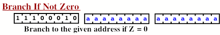
This instruction will branch to the address given in the instruction if the “zero” condition code bit is clear (i.e., is zero). In other words, it will jump if the last ALU instruction (i.e., ADD, INC, AND, OR, XOR, NOT, or SHL) produced a result that was not zero, and not jump otherwise.
Since this instruction can be used in equality tests, it is sometimes called the “BNE” (i.e., Branch-If-Not-Equal) instruction.
Assembly Language / Assembler
There is no official assembler or assembly language for this computer, although several people have created some. Instead, the programs I’ve written have been written in an informal assembly language and have then been hand-assembled into machine code.
An Example Program
This computer does not contain a subtract instruction. Below is a program that subtracts two numbers:
Address Instruction
0000 0000 1000 0101 A = NOT B
0000 0001 0000 1000 B = A
0000 0010 1000 0001 A = B+1
0000 0011 0000 1000 B = A
0000 0100 1000 0000 A = B+C
0000 0101 1010 1110 HALT
This program assumes the two numbers to be subtracted have been pre-loaded into the B and C registers. This program sets
A = C - B
For example:
C: 1001 1101 157
B: 0101 1001 - 89
A: 0100 0100 68
For more complex programs, I’ve adopted a slightly different form in which to express the code. On each line you’ll see the instruction expressed (1) in machine code, (2) in assembly-like code, and (3) in higher-level pseudo-code. For example:
Address Instruction
...
... ... ...
0010 0001 0000 1111 B=Y if sign(Y)=1
0010 0010 1000 0101 A=¬B .
0010 0011 1111 0000 BNEG Lab2 .
0010 0100 0000 0000 . .
0010 0101 0011 0000 . .
0010 0110 0000 1101 B=M2 M2 = M2 + X
0010 0111 0001 0110 C=X .
0010 1000 1000 0000 A=B+C .
0010 1001 0010 1000 M2=A .
0010 1010 1110 1000 BNC Lab2 if carry
0010 1011 0000 0000 .
.
0010 1100 0011 0000 . .
0010 1101 0000 1100 B=M1 M1 =
M1 + 1
0010 1110 1000 0001 A=B+1 .
0010 1111 0010 0000 M1=A .
0011 0000 0000 1011 Lab2: B=D D = D + 1
0011 0001 1000 1001 D=B+1 .
...
... ... ...
Other example programs are available on the website. These programs have been typed into simple text files. They have been hand-assembled, which means the machine code bits have been produced manually, when pencil, paper, and care.
Each program has been run and tested. A program is loaded into memory bit-by-bit, by flipping switches on the computer’s front panel.
Physical Organization of the Computer
The computer consists of four major functional units:
The Arithmetic Logic Unit (ALU)
The Register Unit
The Program Control Unit
The Sequencer Unit
Each unit is housed in a separate mahogany cabinet. Each cabinet has a clear acrylic front panel, which is 26” wide by 38” high.
Each cabinet consists of 4 mahogany boards mitered at the corners, with a routed grove to accept the acrylic front panel. The back of each unit consists of a 1/4” white melamine board and there is another routed grove in the mahogany boards to accept the backboard. The side boards are fastened permanently to the bottom board, but the top board is held in place by removable screws. Therefore, the top of each unit can be removed and the acyclic front panel can be slid into (or out of) the cabinet. Also, the backboard can also be slid into (or out of) place.
Each acrylic front panel has a number of pre-drilled holes, to accept switches, LEDs, and bolts. All external wires exit the cabinet through holes drilled in the mahogany sides. Nothing is attached to the backboards, except a small thermometer. The computer consumes quite a bit of power, which is converted to heat trapped within the cabinets and the thermometers monitor the temperature near the top of the cabinets.
Each cabinet also has a small fan mounted inside, on the bottom board. There are two vents in each cabinet: one directly below the fan and one on the cabinet top. Air is sucked in the bottom by the fan and exits through the top vent. The vents are trimmed out with chrome plates, which hold filter fabric in place to prevent dust / insect accumulation inside the cabinets.
The benefit of allowing the front panel to slide into place is that it can be assembled in isolation and, when completed, it can be slid into the cabinet. When loaded with relays, wire and switches, the front panels are heavy enough to be quite awkward. Also, after the fan wires and external wires have been connected, removal of the front panels is a hassle. The benefit of allowing the back panel to slide out is that the back panel can be easily removed to install / debug / repair the circuitry.
The ALU was constructed by first gluing the relays directly to the acrylic front panel, and then soldering the wires into place. Unfortunately, the size of the acrylic (26” by 38”) was large enough to make soldering and testing inconvenient. A lot of soldering was involved and you don’t want to do this with your arms stretched over such a large area.
The other three units each utilize smaller “modules.” Each module is also made of clear acrylic. The relays were glued directly onto the smaller acrylic modules and then most of the wires were soldered into place. Then, the module was screwed to the front panel, using nuts and bolts and plastic spacers.
For example, each register module uses of a piece of acrylic 3.5” high by 18” wide. After being completed, each of the acrylic modules was secured to the front panel. Each module has 4 holes for mounting bolts in each of the 4 corners, inset by 1/2”. Each register module has between 12 and 16 relays and 8 LEDs. This module size worked well in practice.
When complete, each module was bolted to a front panel and the wires from the module were connected with other wires from other modules using “butt splices.”
A butt splice is a simple, inexpensive and reliable solution to connecting 2 or more wires. A butt splice is basically a tube of soft metal, covered with a tough insulating plastic. To use a butt splice, you insert the end of a stripped wire into one end and, using a crimping tool, crush the metal tube around the wire. Then you insert another wire into the other end and crimp it.
The butt splices were quick to attach. Also, circuits could be altered easily, if mistakes were made. To repair a mis-wired circuit, you simply cut the wires at the bad splice, discard the used splice, re-strip the wires, and install another butt splice. If a wire turns out to be too short, which happened a couple of times, I used an extra butt splice to add an extension wire.
To attach more than two wires to each other, you can strip 2 or 3 wires, twist them together, then insert them into one end of a butt splice and crimp them all together. With three wires going into one end of a butt splice and three wires in the other end, you can connect up to 6 wires. For the cases requiring more connections, you’ll need to break it into multiple butt splices.
Each of the register modules contains a single LED for each of the 8 bits in the register, showing the value stored in the register. The LEDs I used are inserted into a 9/32” hole from the outside and secured using a nut from the inside.
The acrylic of each module is kept about 1/4” from the front panel acrylic by small plastic spacers. The corner of each module is secured to the front panel with a nut, bolt, spacer, and a couple of washers.
One problem with this approach is that it is impossible to replace an LED without unbolting and removing the module. Unfortunately, once the module has been installed, and all the wires to other modules have been connected, it is very difficult to pull the module out far enough to extract a faulty LED. Consequently, I tested all LEDs before installing the module.
The only LED failures I encountered were caused by physical destruction from over-tightening the nut, although a couple LEDs were dim enough to merit replacement.
Parts List and Costs
Relays. The computer contains 415 relays, although I used a several more for prototyping and testing. Each relay is the identical part and each is a 4-pole, double throw relay, rated at 12 volts. [Details: All Electronics Corp; 1-888-826-5432; http://www.allelectronics.com; 4PDT 12 volts DC KH Style; Omron # MY4 DC12, 160 ohm coil. 4PDT contacts rated 5 Amps @ 240 Vac/ 28 Vdc. Solder or socket mount terminals; UL, CSA; Catalog number 4PRLY-12; Price: $3.75 each in quantities of 10 to 99 ($3.40 each in larger quantities); in stock, ships within 24-48 hours. (I used solder terminals. I considered using sockets, but sockets would have added additional cost, more work, and more potential failure points.)]
Switches. The computer contains 111 single-pole, double-throw ON-ON mini toggle switches, although more were used in prototyping, test harnesses, and lost to failure. [Details: All Electronics, catalog number MTS-4, solder terminals, $0.90 in quantities of 10-90.] If I had it to do again, I would order a better switch. I have had several switches fall apart from physical stress. Also, I would choose a switch with a wider paddle, since the little things can cut into your fingers after extended periods of toggling in program code!
LEDs. The computer contains 350 LEDs, although more were used in prototyping, test harnesses, and lost to failure. The part I selected does not require a separate resistor and is meant as a indicator light so they are fairly bright. [Details: Radio Shack; 1-800-THE-SHACK (1-800-843-7422); Part number 276-270; $1.49 each; 12mA.]
Acrylic Boards. The computer contains 4 front panel acrylic boards and several smaller pieces of acrylic for the modules. Here is a break down of the individual pieces of acrylic along with their sizes. All are 1/4” thick.
ALU Unit: 38” high by 26” wide
Register Unit: 38” high by 26” wide
Program Control Unit: 38” high by 26” wide
Sequencer Unit: 38” high by 26” wide
(16) Registers: 3.5” high by 18” wide
Clock: 3.5” high by 13” wide (4 relays, 4 LEDs)
State Sequencing: 6.5” high by 18” wide (31 relays, 28 LEDs)
Instruction Decoding: 10” high by 22” wide (approx 50 relays, 42 LEDs)
Main Memory: 9” high by 22” wide (37 relays, no LEDs)
The module boards have holes for LEDs and mounting bolts. The front panels have holes for LEDs, mounting bolts, and switches.
The acrylic was special-ordered from a local plastics fabricator. All pieces were cut to order and all holes were predrilled. The total cost of acrylic was about $1,095, or about $275 for each of the 4 units.
12 Volt Power. The main power is supplied by two 10 Amp, 12 volt regulated power supplies. These are wired in parallel. [Details: Radio Shack; Part number: 22-506; $79.99 each.]
Wire. Most of the wire in the computer is 22-guage solid copper wire with black insulation. I estimate approximately 2000 feet were used. [Details: Radio Shack; $4.49 per 100 foot spool.] In addition, 18 gauge was used for power and ground within each unit.
Inter-Unit Cables. Between the units there are several cables. Each cable has 8 conductors. The cable is sold as CAT-5e cabling (for Ethernet use) and consists of 4 twisted pairs of 24-guage solid core. [Details: 1 spool of 328 feet at $42.00 is more than you’ll ever need.]
Cable Connectors. Each unit can be disconnected from the rest of the computer, which is essential for moving the computer. The cables are connected using DB-9 sub-miniature connectors. There are 32 male plugs ($1.59 each), 32 female receptacles ($1.79 each) and 64 connector hood cases ($0.45 each). These were somewhat tedious to assemble and I think there must be a better solution.
Fans. Each unit contains a 12 volt cooling fan. [Details: Radio Shack, part number 273-239; 110mA; 14.5 CFM (cubic feet/minute); $10 each.]
Capacitors. The clock circuit utilizes 4 capacitor groups of 500UF each. Each capacitor group contains 5 capacitors of 100 UF each, wired in parallel. Thus, are 20 capacitors total. [Details: 100UF, 100 volts, non-polar, $1.55 each; All Electronics, 800-826-5432; www.allelectronics.com; part number NC-100.] The static memory chip also uses a smaller capacitor across its power and ground. The relays generate a lot of electrical noise and the memory chip was totally unreliable without this capacitor.
Memory Board. The memory board contains 1 SRAM chip, 1 eight-channel FET driver, 3 eight-channel LEDs, all mounted on a 5” by 7” prototyping board. In addition there is a small 5 volt power supply for the chip.
SRAM Chip. The memory is implemented with one static RAM chip providing 32K by 8 bits of storage. [Details: Jameco Electronics; 650-592-8097; catalog number 82472CA, Other part number: 62256LP-70; price: $5.49).]
FET Driver Module. The SRAM chip is not powerful enough to drive a relay; therefore a single eight-channel FET driver module provides 8 amplifiers that will convert from TTL levels to drive the relays. [Details: NCD, www.controlanything.com, part number: 8-FET; price: $49.00.]
Micro-sized LED Arrays. Mounted next to the SRAM chip are 3 eight-channel LED arrays. One monitors the 8 data lines to/from the chip. The other two arrays monitor the 15 address lines to the chip. [Details: NCD, www.controlanything.com, part number: IOTEST-L; price: $10.00.]
5 Volt Power. In addition to the 12 volt power supply, there is a small power supply for the memory chip and associated circuitry. [Details: 5V, 4 Amp, 20 Watt, Jameco catalog number: 213583CA, price: $26.95.]
Power Switch. There is also a power switch, which switches 110 volt line current. The power switch is mounted in the sequencer unit. An external line cord with a plug on one end is routed into the sequencer unit to the power switch. From there, one branch goes back out of the sequencer unit to a receptacle, which was actually the female end of a utility extension cord. The two 12 volt power supplies are plugged into this receptacle, allowing the power supplies to be disconnected for transportation. The other branch from the power switch goes to the small 5 volt power supply, which is inside the sequencer unit.
Cabinetry. The computer is housed in 4 mahogany cabinets, with dark stain and varnish. These were made by a cabinet maker for about $300 each. Each cabinet has 4 rubber feet on the bottom, so that the computer can stand on a long table. In addition, each cabinet has very sturdy picture hanging hardware secured to the back of the side boards, so that the computer can be hung on a wall. The attachment from the cabinet bottom to the cabinet side is reinforced with a metal L-brace so that the weight of the acrylic doesn’t cause the bottom board to separate from the side boards, when the unit is hanging on the wall. Currently, the computer hangs on the wall in my office, with power supply on the floor underneath.
Total Cost. Here is a rough breakdown of the cost of building the computer.
|
1,411 |
Relays |
|
521 |
LEDs |
|
100 |
Switches |
|
1,095 |
Acrylic Boards |
|
1,200 |
Cabinets |
|
160 |
Power Supplies |
|
117 |
SRAM Memory |
|
148 |
Capacitors |
|
138 |
Connectors |
|
132 |
Wire |
|
20 |
Fans |
|
100 |
Misc. Hardware |
The grand total comes to about $5,142, which is about $1,285 per unit.
Concluding Remarks
Building this computer was a
tremendously rewarding project for me.
I have, in my life, written some very complex software which, in terms
of complexity of design and effort of construction, dwarfs this computer. But my friends and family can look at
this physical object and see something that seem understandable, accessible, or
at least interesting and attractive.
This has been very satisfying.
As a young boy, I dreamt of
building a computer out of relays after my father brought home some old,
worn-out relays from a decommissioned telephone switching station. I made a few attempts at the time, but
soon gave up. After finally
realizing this dream many years later, I felt as if I had completed an
unfinished task that had been in the back of my mind all my life, like
something on your to-do list that never gets done but keeps nagging at your
subconscious. I felt joy at
crossing this life-goal off my list!
Building complex machines is an
excellent way to learn about how things work. You always want to attempt to build something that seems
right at the edge of—or just beyond—your capabilities. You always want to risk failure,
because that is when you can learn and grow. When you succeed at getting something to work that you
weren’t sure of, you’ll be proud indeed.
I heartily encourage you to build
your own relay computer. I hope
that this description has given you some ideas that you can use in your design.