Microwave Circuit Design: Lab 6
© B. Pejcinovic, P. Wong, O. Woywode
Introduction
This lab looks at the design process behind a simple two-port
negative-resistance oscillator circuit. Special procedures for
testing and simulating oscillator circuits in MDS are also introduced.
Design Specifications

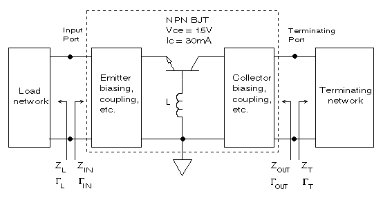
Figure 1: Block diagram of an oscillator using
a BJT
You are to construct an oscillator circuit that has a fundamental
oscillation frequency of fosc = 3 GHz. The original
circuit, along with explanatory notes, can be found on pages 446-448
in the textbook "Microwave Transistor Amplifiers, 2nd
Edition".
The core of the oscillator is an NPN bipolar junction transistor
(BJT) in common-base configuration. In MDS, you can choose transistors
that use either linear models or nonlinear models. The linear
models are suitable for linear, small-signal applications. However,
oscillator circuits assume large-signals and are highly nonlinear
by nature. Hence, a nonlinear transistor model is needed in order
to accurately simulate the behavior of the oscillator. MDS has
a default nonlinear BJT model that you may use for your circuit.
The default model will require a few parameter modifications to
work properly.
The nonlinear BJT device is not self-biased, so you will need
to add DC bias circuits in order to power the oscillator. Fortunately,
the bias networks are already provided in the textbook, so you
will not have to design them.
In Figure 1, Gamma_T and ZT are the terminating
reflection coefficient and terminating impedance, respectively.
Also, Gamma_L and ZL are the load reflection
coefficient and load impedance, respectively. Gamma_IN is the
reflection coefficient looking into the input port of the BJT
circuit (which includes the bias circuits).
Design Approach
To keep the lab simple, the following procedure will be used:
- Select a transistor that is potentially unstable at the frequency
of oscillation.
- Choose a Gamma_T for the terminating network that will make
|Gamma_IN| > 1,
where Gamma_IN = (S11 -
delta*Gamma_T) / (1 - S22*Gamma_T).
- Calculate Gamma_L for the load network that will resonate
ZIN at the oscillation frequency.
If ZIN = RIN + jXIN,
then ZL = RL + jXL
where RL = |RIN| / 3 and XL
= - XIN.
BJT Circuit Characteristics
Assignment
In this section, you will determine the characteristics of the
NPN BJT. In order to get valid results, the transistor should
be operating at its designed bias point, so the DC bias networks
must be in place.
Circuit construction

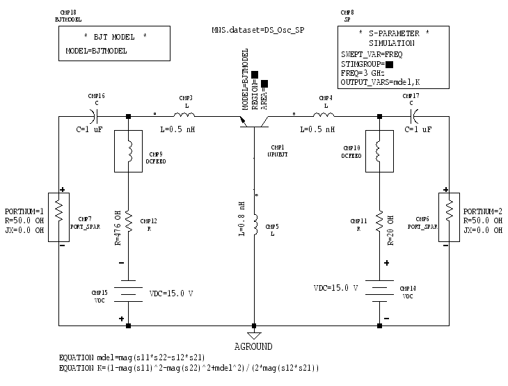
Figure 2: Characterization test circuit
The NPN BJT is configured for common-base operation. The transistor
has a MODEL parameter that specifies the name of the BJT
model to be used in the simulation. The MODEL parameter
only specifies the model name, but does not define the
model parameters.
To actually define the parameters in the nonlinear BJT model,
you have to insert a model component onto the circuit page. There
are two ways to do this:
- BJTMODEL component
This component looks like a small box with the label *
BJT MODEL * and a single parameter called MODEL. There
are no other visible parameters in the box. The MODEL parameter
should be set to the same name you specified for the BJT. To edit
the model parameters, you need to select the component and then
choose [MB:PERFORM/EDIT COMPONENT]. MDS will then open a new dialog
window that displays all of the model parameters that you can
change.
The main advantages of the BJTMODEL component are that it hides
the details of the model and uses the least amount of space on
the circuit page. For all of the schematics shown in this lab,
the BJTMODEL approach is used exclusively.
- BJTMODELFORM component
This component is a big rectangular box with the label *
BJT MODEL * and the parameter MODEL (which should be
set to the same name you specified for the BJT). Also within the
box is a list of all the model parameters that you can edit.
The principal advantage of using BJTMODELFORM is that every model
parameter is visible at all times, so changing a value here or
there is easy. Of course, the major disadvantage is that the form
takes up a lot space on the circuit page.
The schematic on page 446 of your textbook is incorrect
because it has both model components on the same circuit page.
You may choose either model component (the effect is the same),
but do not use both of them simultaneously (at least not with
the same names).
The DCFEEDs, resistors, and DC voltage supplies form the bias
networks for the transistor (VCE = 15 V and
IC = 30 mA). The capacitors block DC from reaching
the S-ports. Attached to the BJT's collector and emitter
are 0.5 nH inductors, which model the inductance of the lead wires.
The inductor connected to the base of the BJT provides feedback
that enhances the instability of the transistor. At the bottom
of the figure are equations for computing the stability factor
K and the magnitude of delta.
In the upper right corner of the figure is a control box for performing
an S-parameter simulation. You will use this control instead
of accessing the standard 'Simulation Setup' dialog window.
- Construct the circuit shown in Figure 2.
- To access the NPN BJT, click [MB:INSERT/MDS COMPONENTS/NONLINEAR
DEVICES/BJT/NPN DEVICE]. Set MODEL=BJTMODEL next to the
transistor.
- The DCFEED, resistor, capacitor, and inductor components are
all located in the same lumped component menu/palette.
- To get the BJTMODEL box, choose [MB:INSERT/MDS COMPONENTS/NONLINEAR
DEVICES/BJT/MODEL]. Position the box and click the left mouse
button to drop it. Select the BJTMODEL box by clicking on it and
use [MB:PERFORM/EDIT COMPONENT] to access the model parameters.
These are the values you need to set (see page 446 of the textbook):
BF=150, VAF=75, TF=30p, BR=1, TR=75n,
IS=2p
CJC=1.5 pF, VJC=0.75, MJC=0.5, CJE=1.5
pF, VJE=0.75, MJE=0.5
RB=5, RE=1, RC=3
If you prefer to use the BJTMODELFORM box instead, choose [MB:INSERT/MDS
COMPONENTS/NONLINEAR DEVICES/BJT/MODEL FORM] and enter the required
parameter values directly into the form.
- To place the S-parameter simulation control box on
the circuit page, choose [MB:INSERT/MDS CONTROL/ANALYSIS/S PARAMETER/SMALL-SIGNAL].
Erase any value next to the STIMGROUP parameter. Set the
FREQ parameter to 3 GHz. Define the equation variables
K and mdel as output variables by listing them next
to the OUTPUT_VARS parameter.
- The MNS.dataset= line defines the name of the dataset
that will hold the results of the simulation. Use [MB:INSERT/MNS/DATASET
NAME] to place the line onto the circuit page. You can use whatever
name you wish, as long as you remember to use the same dataset
name for your presentation page.
Simulation
- Highlight the control box labeled * S-PARAMETER SIMULATION
* by clicking it. Start the simulation by clicking the [S]
button on the left side of the circuit page window.
Output
- Use a template to create a tabular listing of the S-parameters.
Add listing columns for K and mdel.
- Using the techniques of the previous lab (refer to Lab
5: Amplifier Design for Noise), create a blank Smith chart
on the same presentation page as the S-parameter listings.
Insert a trace for the load stability circle, which defines the
allowable values of Gamma_T. Insert another trace for the source
stability circle, which defines the permitted values of Gamma_L.
(It sounds backwards, but that is how Figure 1 defines the oscillator
circuit's terminating and load networks.)
Identify and label the unstable regions of the Smith chart
for Gamma_T and Gamma_L.
Items to turn in
- Turn in a printout of the characterization circuit.
- Submit a printout of the S-parameters and stability
circles.
Questions
- At a frequency of 3 GHz, what is the stability of the BJT
circuit (with its bias networks, etc.)? Justify your conclusion.
Pay particular attention to the S-parameter, K,
and |delta| values.
- From the stability circle data, are there any restrictions
on the choice of either Gamma_T or Gamma_L?
- The textbook suggests using Gamma_T = 0.8 | 70 degrees
for the terminating network. Does that particular reflection coefficient
fall within an unstable region?
BJT Circuit Stability vs. Base Inductance
Assignment
You will examine the influence of the BJT's base inductor on the
stability of the BJT circuit.
Circuit construction
- The stability versus base inductance test circuit is identical
to the circuit in Figure 2. You do not have to make any changes.
Simulation
- Configure MDS for an S-parameter simulation using the
'Simulation Setup' dialog window (you won't be using the S-parameter
control box this time). Set MDS for a single point sweep at 3
GHz. From the dialog window, change the dataset name to prevent
overwriting any previously saved data.
- Next, initialize a parameter sweep of the feedback inductor's
L value. Set the sweep range from 0.0 to 1.0 nH in 0.l
nH steps (use the "nano" multiplier). Now run the simulation.
Output
- Plot both |S11| and |S22|
versus L on a single graph. On a separate graph, plot K
and |delta| versus L.
Items to turn in
- Turn in the presentation page with the S-parameter
vs. L and stability factors vs. L graphs.
Questions
- The circuit in the textbook uses L = 0.8 nH for the
base inductor. From your plots, explain why this inductance value
is a reasonable choice.
Load Network Calculations
Assignment
In this section, you will determine Gamma_IN from Gamma_T. Once
Gamma_IN is known, you can then compute the required Gamma_L for
the load network.
Calculations
- As mentioned earlier, the textbook suggests using Gamma_T
= 0.8 | 70 degrees because
it is a "convenient" value for the terminating reflection
coefficient. From your prior stability circle work, there are
clearly many possible choices for Gamma_T that may lead to oscillation.
How the author settled on that particular value of Gamma_T is
somewhat unclear, but we will assume that there was a logical
reason for doing so. Hence, use the textbook value for Gamma_T
in your design calculations.
- Once the value of Gamma_T has been fixed, Gamma_IN can be
found from the equation:
Gamma_IN = (S11 - delta*Gamma_T) / (1 - S22*Gamma_T).
Using the S-parameters computed by MDS for the BJT circuit,
calculate Gamma_IN and express the answer in magnitude and phase
format.
- With the results of the previous step, compute Gamma_L and
write the solution in magnitude and phase format. Also calculate
the equivalent unnormalized load impedance ZL.
Items to turn in
- Submit your calculations for Gamma_IN, Gamma_L, and ZL.
Questions
- Does the computed Gamma_L value fall within an unstable region
on the Smith chart?
Verifying Gamma_IN Using MDS
Assignment
You will use MDS to experimentally find Gamma_IN and then compare
its value to your calculated Gamma_IN.
Circuit construction

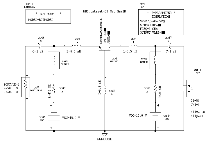
Figure 3: Gamma_IN test circuit
This is essentially the same circuit as in Figure 2, but the S-port
on the terminating port has been replaced by a special component
labeled S1P. S1P is a single port device that presents
a fixed reflection coefficient at its input terminals. This allows
you to easily insert a terminating network without worrying about
the actual implementation details.
- Construct the circuit shown in Figure 3.
- Use [MB:INSERT/MDS COMPONENTS/LINEAR DEVICES/MODEL/ONE PORT/S
MAG PHASE] to access the S1P component.
Set Z1=50 and JX1=0. This tells MDS that the S1P
port impedance is 50 ohms (remember that your S-parameter
measurements used 50 ohm ports).
Set S11m=0.8 and S11p=70. This forces the reflection
coefficient presented at the terminals of S1P to be 0.8 | 70
degrees. A nice feature of the S1P component is that the reflection
coefficient is fixed and won't change even if the frequency shifts
(which is a definite problem for networks built from discrete
elements or microstrip).
Don't confuse the S11m and S11p parameters with
the normal S-parameters that MDS computes. S11m
and S11p refer only to the S1P component and have
nothing to do with S-parameters elsewhere in the circuit.
Simulation
- Highlight the control box labeled * S-PARAMETER SIMULATION
* by clicking it. Start the simulation by clicking the [S]
button on the left side of the circuit page window.
Output
- Record the magnitude and phase of S11 at
the input port of the BJT circuit.
Items to turn in
- There are no formal presentation pages to turn in. However,
state your recorded S11.
Questions
- For the circuit in Figure 3, Gamma_IN = S11.
Does the simulation value for Gamma_IN match your manually calculated
value?
Basic Oscillator Tests
Assignment
You will test the oscillator circuit to determine whether or not
it has the potential to oscillate.
Circuit construction

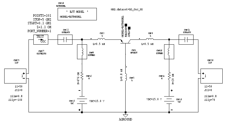
Figure 4: Oscillator test circuit (OSCTESTG - Nyquist
diagram)
The circuit in Figure 4 is similar to the one in Figure 3, with
four major exceptions:
- The * S-PARAMETER SIMULATION * control box is omitted.
- The 1 uF blocking capacitors are replaced by DCBLOCK components.
- The S-port that was on the input port of the BJT circuit
is replaced by an S1P component (to simulate the load network).
- A new device labeled OSCTESTG is inserted in the circuit.
It is a probe that measures the open-loop gain and phase of the
closed-loop system. By plotting the results on a polar graph (Nyquist
diagram), you can determine if the circuit has the potential to
oscillate.
Note that the OSCTESTG probe only checks whether or not the circuit
satisfies certain oscillation conditions. It does not actually
solve the nonlinear equations necessary to simulate the oscillation
behavior of the circuit.
- Construct the circuit shown in Figure 4.
- The load network S1P component is initially set up for Gamma_L
= 0.8 | -144 degrees, which is the non-optimized value
mentioned in the textbook. Instead of using that value, edit the
S11m and S11p parameters to use the Gamma_L value
you computed in the calculations section of the lab.
- For negative resistance oscillators, OSCTESTG is inserted
between a negative and positive impedance in the circuit.
Choose [MB:INSERT/MDS CONTROL/ANALYSIS/S PARAM OSC TEST] to insert
the OSCTESTG probe.
Set PORT_NUM=1 to have MDS test S11.
The Z parameter is the initial probe impedance and should
be about a factor of five lower than the magnitude of the passive
load impedance. You can use the default value of Z=1.1
OH.
Set START=0.1 GHz, STOP=5 GHz, and POINTS=101.
This tells MDS the range of frequencies you want tested for possible
oscillation.
Simulation
- Highlight the OSCTESTG probe by clicking it. Start the simulation
by clicking the [S] button on the left side of the circuit page
window.
Output
- On a single graph, plot the magnitude and phase of S11
versus the frequency. Both axes should be on a linear scale. Adjust
the limits of the y-axis to make the horizontal grid line running
through the center of the graph represent zero magnitude and zero
phase.
Frequencies at which the phase of S11 goes to
zero correspond to possible frequencies of oscillation. Depending
on the OSCTESTG frequency search range, there may be multiple
zero phase crossings. At each zero phase crossing, if |S11|
> 1 then the circuit has the potential to oscillate at that
frequency. If |S11| < 1, then the open-loop
gain is less than unity and the circuit will not oscillate at
that frequency.
>From your graph, locate the frequency at which the phase of S11
is zero. Now examine the magnitude of S11 at
that same frequency. You can get better accuracy by inserting
markers on the phase and magnitude traces.
- On the same presentation page, create a Nyquist diagram by
making a polar plot of S11.
If a circuit is capable of oscillating, then the S11
curve must make a clockwise track on the polar plot as the search
frequency increases, and the curve must encircle the point 1 +
j0 (the unity gain point).
Insert a marker on the S11 curve. Move the marker
along the S11 trace until you reach the positive
real x-axis (i.e., imaginary coordinate is zero). The marker display
will tell you the magnitude of S11 and the frequency
at that point.
Items to turn in
- Turn in the plot containing the S11 vs.
frequency (LIN-LIN) graph and the Nyquist diagram.
Questions
- From your plot information, what is the potential oscillation
frequency?
Oscillator Harmonic Balance Test
Assignment
The OSCTESTG probe of the previous section is useful for performing
certain linear tests that examine the potential for oscillation.
However, OSCTESTG cannot test the oscillation behavior itself,
since that requires a nonlinear simulation. To actually test the
oscillation mode of the circuit, you will perform a nonlinear
simulation using the technique of harmonic balance.
Harmonic balance simulation
The nonlinear oscillator simulation tool is the OSCPORTG component,
which is inserted into the oscillator circuit to perform a harmonic
balance test. In a harmonic balance analysis, a frequency spectrum
is built from individual sinusoids, which are then applied simultaneously
to the circuit being simulated. The magnitudes and phases of the
sinusoids are the Fourier coefficients of the corresponding time-domain
waveform. After a harmonic balance analysis is performed, the
result is a set of voltage and current spectra for each node and
component in the circuit. Because the nonlinear analysis makes
fewer assumptions on waveform behavior than does linear analysis,
the results are more rigorous. Since the final loop gain of the
oscillator depends on the steady state large signal amplitude,
harmonic balance provides a more accurate picture of the oscillator's
actual performance.
Circuit construction

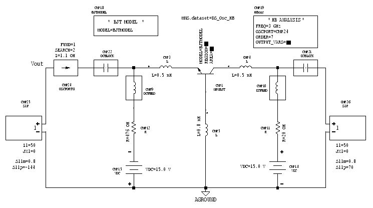
Figure 5: Oscillator test circuit (OSCPORTG - Harmonic
balance)
The harmonic balance test circuit in Figure 5 is similar to the
Nyquist test circuit of Figure 4, with two exceptions:
- The * HB ANALYSIS * control box is added.
- The OSCPORTG component replaces the OSCTESTG device.
- Construct the circuit shown in Figure 5.
- For the load network S1P component, edit the S11m and
S11p parameters to use the Gamma_L value you computed in
the calculations section of the lab.
- For output plotting purposes, you need to identify the voltage
output node of the oscillator circuit. The required node is located
between the S1P and the OSCPORTG components and is labeled as
Vout on the schematic.
To label the node, choose [MB:INSERT/WIRE/LABEL]. An outline of
a tiny box connected to crosshairs (that looks like an "X")
tags along with the mouse pointer. Position the crosshairs somewhere
on the wire that joins the S1P and OSCPORTG components and click
the left mouse button to drop the label. Click inside the tiny
blue box to edit it, and type Vout.
- Choose [MB:INSERT/MDS_COMPONENTS/PROBES/OSCPORT GROUNDED]
to access the OSCPORTG component.
Z is the initial probe impedance, SEARCH is the
number of octaves to search, and FUND is the fundamental
number for the oscillator. Use the default values.
- Choose [MB:INSERT/MDS CONTROL/ANALYSIS/HARMONIC BALANCE/OSCILLATOR]
to insert the * HB ANALYSIS * control box.
FREQ is the initial guess for the oscillation frequency.
Set FREQ=3 GHz.
The OSCPORT parameter identifies which OSCPORTG is to be
used for the analysis. Suppose CMP# is the component number
of OSCPORTG in your own circuit. Set OSCPORT=CMP#.
The ORDER parameter sets the upper limit on the number
of harmonics computed. Set ORDER=7.
Simulation
- Highlight the * HB ANALYSIS * control box by clicking
it. Start the simulation by clicking the [S] button on the left
side of the circuit page window.
- If your oscillator schematic is correct, then the harmonic
balance analysis should be successful. If the simulation fails,
the resulting error message will probably be very cryptic and
not of much help. If that happens, look over your circuit very
carefully to find the problem and then re-run the harmonic balance
analysis.
Output
- On a new presentation page, create these three plots:
Spectrum vs. Harmonic Index
Choose [MB:INSERT/TEMPLATE/templatelib/Harmonic_Balance/Spectrum].
Position the outline of the template on the presentation page
and click the left mouse button to drop the template. MDS then
displays the power spectrum (in dB) at the Vout circuit
node versus the harmonic index.
Spectrum vs. Frequency
Use [MB:INSERT/TEMPLATE/templatelib/Harmonic_Balance/Spectrum]
to insert another spectrum plot. Click inside the x-axis label
and change it from harmindex to freq. MDS will redraw
the spectrum plot as a function of frequency. If necessary, perform
an autoscale on the axes to get a nice looking plot. Add a marker
to the spectrum trace. Move the marker to the first spectral line
to identify the fundamental (first harmonic) oscillation frequency.
Waveform vs. Time
Choose [MB:INSERT/TEMPLATE/templatelib/Harmonic_Balance/Waveform].
Position the outline of the template on the presentation page
and click the left mouse button to drop the template. MDS then
displays the voltage waveform (in volts) at the Vout circuit
node versus time (in seconds).
- On the same presentation page, add a listing column. The column
heading should be changed to "freq[2]", which is where
the first harmonic frequency is stored.
Items to turn in
- Submit a printout of the harmonic balance test circuit.
- Turn in a printout of the spectrum/waveform plots and the
frequency listing.
Questions
- From the spectrum plot data, what is the fundamental oscillation
frequency of the circuit? What is the percentage difference between
the frequency computed by harmonic balance and the design value
of 3 GHz?
Note: You may have realized that the potential oscillation
frequency predicted by OSCTESTG was relatively far away from the
actual oscillation frequency. This should reinforce the idea that
the linear open-loop gain/phase plots should serve only as a rough
guide to the behavior of the oscillator.
- It is evident that the voltage waveform at the output node
is sinusoidal, but there is also a distinct "kink" in
the waveform. What do you think is causing this effect? (Hint:
Look at the higher order harmonics in the spectrum plot.)
Optimization of fosc
Assignment
The fundamental oscillation frequency of the basic oscillator
circuit was close to, but not exactly at the desired frequency
of 3 GHz. You will now apply some optimization techniques to get
a better fit.
Harmonic balance optimization
In the textbook, the author simply states that using the value
Gamma_L = 0.75 | -140 degrees will nudge the oscillation
frequency to 3 GHz. Hence, you need to optimize the S11m
and S11p parameters of the load network S1P component.
In the past, you optimized a circuit by using MDS's built-in
optimization routine. The optimization procedure is a little bit more
involved for this case so you will instaed perform parameter sweeps.
Theoretically, you should perform a two-level nested sweep on
S11m and S11p. To save time and effort on your part,
you are allowed to perform two individual sweeps. That is, hold
S11m fixed at 0.75 and sweep S11p, and then hold
S11p fixed at -140 degrees and sweep S11m. Since
we're already told what the optimal load coefficient should be,
this allows you to see the dependence of the oscillation frequency
on Gamma_L without having to wade through the output from a nested
sweep.
Circuit construction

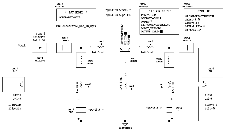
Figure 6: Optimization circuit
Figure 6 is basically the same as Figure 5, with a few critical
additions:
- Equations for SLm and SLp have been added to
define the S11m and S11p values, respectively. This
is necessary because MDS does not allow you to directly access
the S11m and S11p fields of the S1P component for
a parameter sweep.
- The normal * HB ANALYSIS * control box is replaced
by a special swept version.
- A STIMULUS box is added to define the sweep range.
- Construct the circuit in Figure 6.
- Add the equations for SLm and SLp to the circuit
page. For the load network S1P component, set S11m=SLm
and S11p=SLp.
- Choose [MB:INSERT/MDS CONTROL/ANALYSIS/HARMONIC BALANCE/OSCILLATOR
-SWEPT] to insert the swept version of the * HB ANALYSIS *
control box.
Use the same values for the FREQ, OSCPORT, and ORDER
parameters as in the non-swept harmonic balance simulation. Set
SWEPT_VAR to SLm if you want to sweep the magnitude
of Gamma_L, or else set SWEPT_VAR to SLp to sweep
the phase of Gamma_L.
- Choose [MB:INSERT/MDS CONTROL/STIMULUS/START STOP/LINEAR POINTS]
to insert the STIMULUS box.
For a magnitude sweep, set START=0.70, STOP=0.80,
and LINEAR PTS=11.
For a phase sweep, set START= -145, STOP= -135,
and LINEAR PTS=11.
Simulation
- Highlight the * HB ANALYSIS * control box by clicking
it. Start the simulation by clicking the [S] button on the left
side of the circuit page window.
Output
- After the simulation is done, create a new presentation page.
For a magnitude sweep, insert a listing column for SLm.
For a phase sweep, insert a listing column for SLp instead.
Add another listing column to show the oscillation frequency at
each sweep point (do this by setting the column header to "freq[*,2]").
Items to turn in
- Turn in printouts of the listings for fosc
versus the magnitude and phase of Gamma_L.
Questions
- From the sweep data, is Gamma_L = 0.75 | -140 degrees
a good value for the optimal load reflection coefficient?
Terminating and Load Networks
Assignment
In the final section of this lab, you will replace the S1P components
(and their fixed reflection coefficients) with normal circuit
networks (and their frequency dependent reflection coefficients).
The design requirements are fosc = 3 GHz, Gamma_T
= 0.8 | 70 degrees, and Gamma_L = 0.75 | -140 degrees.
Remember that the original S-parameter measurements were
based on 50 ohm port impedances. This means that the terminating
network must transform Gamma_T to 50 ohms, and the load network
must transform Gamma_L to 50 ohms.
You may build the terminating and load networks using either ell
networks or microstrip.
Circuit construction
- Use the circuit shown in Figure 5 as a starting point.
- Delete the S1P components and replace them with terminating
and load networks of your own design. You should tune the reflection
coefficients of the terminating and load networks with the built-in
MDS optimizer before using them in the oscillator circuit.
- IMPORTANT: Delete the DCBLOCK components and replace
them with 0.1 uF capacitors.
For some mysterious reason, the harmonic balance analysis will
fail if you replace the S1P components with normal networks and
retain the DCBLOCK components.
- Make sure the Vout node label is properly located on
the schematic.
Simulation
- Perform a harmonic balance simulation of the completed oscillator
circuit. Use the same analysis settings as in Figure 5.
If the simulation fails (which is possible), then check the design
of your terminating and load networks. Play around with some of
the OSCPORTG and HB analysis parameters to see if that helps.
- Note on optimization: it is possible to perform optimization
that will change specified component values in order to obtain a
specific frequency of oscillation. The procedure is as follows:
Somewhere in your circuit, preferably on the 50 Ohm load, insert
a label "Vout". Set up optimization as usual - you can use the
simulations done above as a starting point.
Then in the optimization goals type in the following:
if mag(v(Vout,1)) >= 0 then get_fund_freq(1) else 0 endif .
This first checks that there are some oscillations, and if there
are it finds the fundamental frequecy. In the entries for range you
can specify the range of frequencies that you will be happy with,
e.g. 2.999 GHz and 3.001 GHz. You can also turn on the "use finite
differences" in gradient optimization parameters which is located
in "OPTIM" window. Don't forget to set up the range of the relevant
components. Try it!
Output
- Make spectrum and waveform plots at the Vout node (like
the ones you made before).
Items to turn in
- Turn in a printout of the oscillator circuit with your own
terminating and load networks in place.
- Turn in the spectrum and waveform plots.
Questions
- What is the oscillation frequency of your circuit? What is
the relative error between the circuit's actual oscillation frequency
and the design frequency?
- Do the power spectrum and voltage waveform look any different
from the results you got using the S1P components?
