EE431/531 Microwave Circuit Design
I: Lab 3
© B. Pejcinovic, P. Wong, O. Woywode
Introduction
This lab delves into the principles of amplifier design under
the constraints of either maximum transducer gain or a specific
operating power gain. In addition, the relationship between constant
gain circles and the frequency is explored. You will also learn
how to create a circuit layout in MDS.
Design Specifications
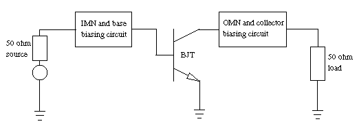
Figure 1: Block diagram of a single stage BJT amplifier
You are to design two different single-stage transistor
amplifier circuits. For the first circuit, the design constraint
is to achieve maximum transducer gain GT,max.
In the second circuit, the amplifier must obtain a specified operating
power gain Gp. The design frequency is f
= 1 GHz.
The input matching network (IMN) and output matching network (OMN)
are to be constructed from microstrip. The substrate is Duroid
(relative permittivity = 2.23 and height H = 0.7874 mm).
The matching networks should use balanced stubs (either
open-circuited or short-circuited) and a series transmission line.
The core of the amplifier is a bipolar junction transistor (BJT)
in common-emitter configuration. For this lab, the transistor
is a Siemens BJT (MDS Part# "siemens_10bfq196_s"). This
particular device is parameterized at a fixed bias of VCE
= 5 V and IC = 70 mA.
Technically, the parameterized BJT does not need external biasing
for simple S-parameter and gain measurements. However,
you are required to design base and collector biasing circuits
(including DC voltage sources) and add them to your amplifier.
You may use high-impedance microstrip, inductors, and capacitors.
Although the bias circuits do not actually power the parameterized
BJT, they may still have an impact on the amplifier due to non-ideal
component effects.
The input port of the BJT needs to be matched to a 50 ohm source,
while the BJT's output port is to be matched to a 50 ohm load.
In the actual circuit, the source and load impedances are represented
by S-ports. Coupling capacitors should be placed between the source
and the IMN, and also between the OMN and the load.
For a good example of what your completed amplifier circuit design
might look like, refer to page 167 of the Gonzalez textbook (2nd
edition).
Circuit Layout
If a circuit design is to be manufactured, then you need to create
a layout for the circuit. The layout procedure converts a schematic
drawing to a set of detailed instructions that tell how to arrange
the circuit for actual fabrication. MDS has layout models for
many circuit components, which are used to define and constrain
the physical layout of the components. For devices with no built-in
models, you can create your own definitions that describe how
to perform the component layout.
In MDS, the layout procedure can be performed automatically or
interactively. In auto-layout mode, MDS examines the schematic,
applies the appropriate models, and then generates the circuit
layout. This is convenient for the engineer, but the resulting
layout might not conform to certain design guidelines (especially
if the models are incomplete). In this case, interactive mode
is appropriate. With the MDS layout editor, you can edit a layout
to fix minor problems or even create new layouts from scratch.
When a circuit layout is produced, MDS creates a layout icon in
the workbench. Double-clicking this icon opens its associated
layout page. What you see on the layout page is a proportionally
scaled view of how the circuit will be constructed.
When the layout is finished, it can be saved as a UNIX file and
imported into special software that validates the layout. Once
verified, the layout can be used as a guide to make PC boards
or IC masks that implement the original circuit design.
Layout problems with the Siemens BJT
The Siemens 10bfq196_s BJT does not have a built-in layout model.
If you attempt to perform an auto-layout of a schematic that contains
the Siemens BJT, MDS will use a default component layout that
makes no sense. To get around this problem, you will define a
new layout model for the BJT.
If package specifications for the Siemens BJT were available,
you could create a realistic layout that takes into account the
actual dimensions of the device. Since we do not have that information,
you will create a simplified BJT layout instead, which consists
of a 70 mil diameter circle with four terminals in the proper
orientation.
Creating a new BJT layout
Here is the procedure for creating the simplified BJT layout:
- Create a new workbench called Lab3
within the MW_Labs project file
(or whatever your project file is called).
- Click [SUI:Layout] to create a new layout. Type 70mil
in the input box of the 'New Layout' dialog window and press RETURN
(or click [OK]). MDS should create a layout icon called 70mil
in the Lab3 workbench.
- The '70mil: DRAWING 1' window appears, along with a 'Momentum'
Palette that pops up on the left side of the screen. You will
not use Momentum for this lab, so you can close the palette window
or simply ignore it. Make sure the layout page is still the active
window.
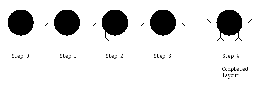
Figure 2: Step-by-step layout procedure for the
Siemens BJT
- STEP 0: Draw the circle (Step 0 of Figure 2).
Choose [MB:INSERT/CIRCLE/BY X-Y VALUES/BY CENTER & RADIUS].
The first dialog window asks for the circle's center, so enter
0,0 in the input box (you
must type the comma between the zeroes). The second dialog window
asks for the radius, so type 35.
The final dialog window asks for the line width. You can just
click [OK]. MDS now draws a filled circle on the layout page.
- STEP 1: Add the first terminal connector (Step 1 of
Figure 2).
Choose [MB:INSERT/CONNECTOR/BY X-Y VALUES]. The first dialog window
asks for an X-Y point pair, so type -35,0
in the input box (remember to type the comma). The next dialog
window wants to know the pin angle, so type 180.
The last dialog window requests a number for the connector. Type
1 in the input box. MDS now
adds the first connector to the circle.
- STEP 2: Add the second terminal connector (Step 2 of
Figure 2).
Repeat Step 1 with these values: (X-Y point pair: -24.7,-24.7),
(Angle: 270), (Number: 2)
- STEP 3: Add the third terminal connector (Step 3 of
Figure 2).
Repeat Step 1 with these values: (X-Y point pair: 35,0),
(Angle: 0), (Number: 3)
- STEP 4: Add the fourth terminal connector (Step 4 of
Figure 2).
Repeat Step 1 with these values: (X-Y point pair: 24.7,-24.7),
(Angle: 270), (Number: 4)
- You have finished creating a simplified BJT layout called
70mil. Close the layout page window.
Accessing the new BJT layout
You have to make a few changes to your circuit schematic in order
to access the simplified layout. Essentially, you insert transistor
attribute statements onto the circuit page which explicitly tell
MDS to use the new 70mil layout
instead of the default component layout. The procedure for doing
this is outlined in the next section.
BJT Characteristics
Assignment
As the first step in the amplifier design, you will determine
the characteristics of the Siemens BJT. From the resulting S-parameter
data, you can instruct MDS to find the reflection coefficients
for a bilateral simultaneous conjugate match and compute the corresponding
maximum transducer gain. The test circuit consists of the BJT,
two S-ports, and no matching or bias networks.
Circuit construction
- In the Lab3 workbench, create
a new circuit page called BJT_char.
Figure 3 shows what your completed circuit should look like.
Figure 3: BJT characterization test circuit
- To access the Siemens BJT, click [Library …] on the Components
Palette. In the Library Browser, click [Select by Type] and choose
the "Select by Library" option. In the left-most panel
of the 'Library Browser' window, scroll down the list and select
the "siemens" option. In the middle panel, select "BFQXXX".
In the right-most panel, select "10bfq196s". Click [OK]
to exit the browser. MDS may tell you that the siemens library
needs to be loaded. Answer "Yes" when prompted.
- Note that the substrate and emitter terminals of the BJT are
attached to global grounds. While functionally similar to analog
grounds, MDS has built-in models for global grounds that are vital
when performing an auto-layout.
To access the global grounds, click [More parts …] on the
Components Palette. From the 'Parts' list window, select the "Global
connectors" option. The Components Palette will then have
an icon with the floating label Gnd, digital. Use that
icon for the global grounds.
- Place S-ports (R = 50.0 OH, JX = 0.0 OH) on
the circuit page. MDS ignores the S-ports when performing a circuit
layout, so they can still use analog grounds.
- Insert EQUATION statements on the circuit page and
edit them to look like Figure 3.
In the first group of equations, K is the stability factor,
mdel is |delta|, U is the unilateral figure of merit,
Gmsg is the maximum stable gain GMSG,
h21ms is |hfe|2, and s21ms
is |S21|2.
In the next group of equations, Gamma_Ms and Gamma_ML
are the source and load reflection coefficients required for a
bilateral simultaneous conjugate match. Finally, GTmax
is the maximum transducer gain GT,max.
MDS's built-in dB function assumes an amplitude ratio for its
argument (i.e., dB(A)=20log(A)). For this lab, a power ratio is
more appropriate (i.e., dB(P)=10log(P)).
Additional EQUATION statements have been defined to do
the proper decibel conversion, and those equation variables (Gmsg_dB,
h21ms_dB, s21ms_dB, and GTmax_dB) are the
correct output variables.
- The layout.leaf and layout.instance statements
are the transistor attribute statements mentioned earlier. They
are not simple text statements. You have to enter them
using an attribute viewer.
Choose [MB:INSERT/ATTR VIEWER]. Although nothing seems to happen,
MDS is waiting for you to select a component whose attributes
you want to change. Select the BJT with the mouse.
A dialog window appears that asks you to insert the attribute
name. Type layout.leaf in
the input box and press RETURN (or click [OK]). A new dialog window
appears and asks if it should create layout.leaf, to which
you should type y in the
input box. The final dialog window asks you to insert the attribute
value for layout.leaf. In the input box, type y.
An outline of the attribute now tags along with the mouse pointer.
Position the pointer where you want the attribute statement to
go and click the mouse to drop it onto the circuit page.
The dialog window that asks for an attribute name automatically
appears again. Repeat the previous procedure to place the layout.instance
statement on the circuit page. Type 70mil
when asked for the attribute's value. To exit the attribute viewer,
click [OK] when the dialog window asking for the attribute name
appears again.
For your information, layout.leaf=y instructs MDS to ignore
the transistor's built-in layout (which the Siemens BJT does not
have anyway). The statement layout.instance=70mil tells
MDS to use an instance of the layout called 70mil,
which happens to contain your simplified BJT layout.
Circuit layout
- Since the test circuit has no matching networks, you do not
have to create a full circuit layout yet.
Simulation and output
- Configure MDS for an S-parameter simulation. Linearly
sweep the frequency from 0.9 to 1.1 GHz with a step size of 10
MHz. In the 'Simulation Setup' window, define the equation variables
K, mdel, U, Gmsg_dB, h21ms_dB,
s21ms_dB, Gamma_Ms, Gamma_ML, and GTmax_dB
as output variables.
IMPORTANT: Change the default dataset name to DS_BJT
before running the simulation.
- After the simulation, create a tabular listing of the S-parameters
versus the frequency. Add listing columns for K, mdel,
and U. Insert additional listing columns for Gamma_Ms
and Gamma_ML (display them in linear magnitude and phase
format). Finally, add a listing column for GTmax_dB.
- Perform another simulation, but this time use a logarithmic
frequency sweep. Set Sweep type to "Log", Start=10
MHz, Stop=6 GHz, and Pts/decade=20.
- Using the new data, make a LIN-LOG plot of Gmsg_dB,
h21ms_dB, and s21ms_dB versus the frequency. They
should all be plotted on the same graph.
Items to turn in
- Turn in a printout of the BJT characterization circuit.
- Submit the listings and the gains versus frequency plot.
Questions
- Is the Siemens 10bfq196_s BJT unconditionally stable at the
design frequency of 1 GHz? From the simulation results, explain
why the transistor does not fulfill the unilateral criterion.
- Discuss the significance of the gains versus frequency plot.
- Determine the frequency at which the transistor becomes potentially
unstable.
- Determine fbeta, fT, and
fs. Explain why you are not asked to find fmax.
(Refer to Fig. 1.11.10 in the textbook for definitions of these
frequencies.)
- What is the maximum transducer gain at the design frequency?
How does GT,max vary with frequency?
Amplifier Circuit 1: Designing for GT,max
Assignment
Using the Gamma_Ms and Gamma_ML values that were
computed in the previous section, design the microstrip input
and output matching networks of the amplifier to achieve maximum
transducer gain (GT,max) at the 1 GHz design
frequency.
Circuit construction
- In the Lab3 workbench, create
a new circuit page called Amp_GTmax.
The circuit you need to build looks like Figure 4 (insert your
own matching networks and bias circuits).
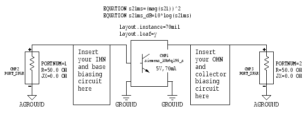
Figure 4: GT,max amplifier circuit
Here are some general hints that may be useful:
- Make a copy of the BJT characterization circuit and use it
as the starting point for your new circuit. Notice that only two
equations are required for the GT,max circuit.
- IMPORTANT: Construct the IMN and OMN as subcircuits.
- Use global grounds in your matching networks and biasing circuits.
- The ideal capacitor component does not have a built-in layout
(MDS uses a default component layout). Try using a chip capacitor
instead, which does have a built-in layout. The ideal inductor
faces the same problem, but there is no readily available alternative.
- The coupling capacitors should provide a low impedance path
for ac signals at the design frequency.
- Since the bias circuits do not really power the parameterized
BJT, the exact values you use in their design are not critical.
However, do make an attempt to choose reasonable values.
Circuit optimization
Before attaching the IMN and OMN subcircuits to the main amplifier
circuit, test them individually first. Verify that the IMN transforms
Gamma_Ms to the 50 ohm source and that the OMN transforms
Gamma_ML to the 50 ohm load.
Use the MDS optimization feature to tune the matching networks
at the design frequency. When you are done, the output port of
the IMN should not deviate more than a few percent from the required
Gamma_Ms value. Likewise, the input port of the OMN should
be as close as possible to the required Gamma_ML value.
Tuning the IMN
- Figure 5 shows the test circuit you need to construct in order
to optimize the IMN.
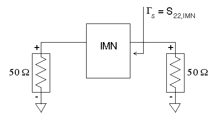
Figure 5: IMN test circuit
- On the output port of the IMN, the required reflection coefficient
is Gamma_Ms, which has a specific magnitude and phase.
For the circuit in Figure 5, notice that by optimizing the value
of S22 (i.e., S[2,2]) at the design frequency,
you are also tuning the value of Gamma_Ms as well.
To tune the IMN, you need to perform a two goal optimization.
The first goal sets limits on the magnitude of S22,
while the second goal sets limits on the phase of S22.
In the goal editor of the optimization setup window, you can enter
multiple design goals, and MDS will try to optimize the circuit
to achieve the desired result. There is no guarantee that MDS
can meet all of the stated goals simultaneously, so you have to
be careful how you define the goals.
Refer to Lab 2 for a reminder of how to access the optimization
feature of MDS. The only thing different in this lab is that you
now have two goals instead of a single goal. By clicking the [Add]
button in the goal editor window, you can enter additional goals.
If you do click [Add], MDS automatically uses the parameters of
the previous goal for your new goal. You can then edit the new
goal and change the settings to what you really want. There are
arrow buttons that allow you to browse forward and backward through
the list of defined goals.
As an example, suppose the required value for Gamma_Ms
is 0.430 |_ -120.5 degrees (use your own computed value). For
the first goal, set Expression="mag(S[2,2])",
Min="0.425", and Max="0.435"
(be careful in choosing your own limits). For the second goal,
set Expression="phase(S[2,2])", Min="-121.0",
and Max="-120.0". For this example, MDS will
try to optimize the circuit parameters (such as microstrip lengths)
to make S[2,2] as close as possible to 0.430 |_ -120.5 degrees.
(Actually, you can also add a goal to optimize S[1,1] so that
its magnitude is near zero. You can try this if you have time.)
- The optimization should be performed at the design frequency
of 1 GHz. After MDS is done, check the computed value of S[2,2]
to see if it meets the goal. If it does, then try making the limits
even tighter for a better match (a relative error of less than
1% or 2% between the circuit's S[2,2] value and the required Gamma_Ms
value is very good). However, don't waste too much time doing
the optimization. Be sure to update your circuit with the optimized
microstrip length values.
IMPORTANT: After you have finished optimizing the IMN,
you need to collect some S-parameter versus frequency data
that will be used later in the lab. Follow this procedure:
- Configure MDS for a standard S-parameter simulation
of the IMN test circuit. Linearly sweep the frequency from 0.9
GHz to 1.1 GHz in 10 MHz steps.
- Change the default dataset name to DS_IMN
before running the simulation.
Tuning the OMN
- Figure 6 shows the test circuit you need to construct in order
to optimize the OMN.
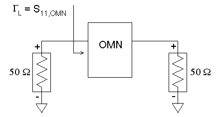
Figure 6: OMN test circuit
- The OMN optimization procedure is basically identical to the
IMN procedure. In this case, you are tuning Gamma_ML by
optimizing S[1,1] on the input port of the OMN. The two goal expressions
are now "mag(S[1,1])" and "phase(S[1,1])".
IMPORTANT: After you have finished optimizing the OMN,
you need to collect some S-parameter versus frequency data
that will be used later in the lab. Follow this procedure:
- Configure MDS for a standard S-parameter simulation
of the OMN test circuit. Linearly sweep the frequency from 0.9
GHz to 1.1 GHz in 10 MHz steps.
- Change the default dataset name to DS_OMN
before running the simulation.
Circuit layout
- Click [SUI:Layout] to create a new layout. Type Amp_GTmax
in the input box of the 'New Layout' dialog window and press RETURN
(or click [OK]). By using a layout name that is identical to the
name of an existing circuit page, MDS will automatically use that
circuit page's schematic when performing the layout.
- The 'Amp_GTmax: DRAWING 1' window appears. Either close the
'Momentum' Palette or else just ignore it. Make sure the layout
page is still the active window.
- Choose [MB:PERFORM/AUTO-LAYOUT]. After a few seconds, the
completed circuit layout will be drawn on the layout page.
- If you find that the circuit layout has a glaring error, correct
the problem and then choose [MB:PERFORM/AUTO-LAYOUT/RE-INSTANTIATE]
to restart the auto-layout process.
Items to turn in
- Include the by-hand Smith charts you used to design the microstrip
matching networks. Explain briefly your design choices. List the
major equations you used.
- Turn in printouts of the main GT,max circuit
and its subcircuits. Also submit a printout of the final circuit
layout.
Amplifier Circuit 1: Using MDS to find GT
vs. freq
Assignment
For the GT,max amplifier circuit, determine
the transducer gain GT as a function of frequency.
Compare GT and GT,max at the
1 GHz design frequency.
GT computation issues
At first glance, calculating the transducer gain using the equations
in the textbook seems like a simple task. However, on closer examination,
there are several subtle points that complicate the situation.
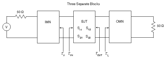
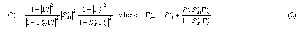
Figure 7: S-parameter and reflection coefficient
definitions for a general amplifier
Figure 7 shows the reference positions for specific reflection
coefficients as defined in the textbook. Notice that S11,
S12, S21, and S22
are the S-parameters for the BJT. The transducer gain formula
is
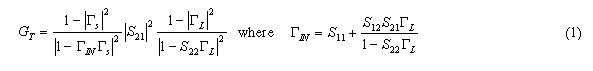
Hence, to compute GT , all you need to do is
plug in the correct S-parameters and values.
So what is the problem? Well, there are actually two potential
difficulties:
- The transducer gain equation is implicitly dependent on the
frequency. For each frequency at which you want to compute GT
, you must re-measure the BJT S-parameters and the reflection
coefficients and then plug those new values into the gain equation.
- In MDS, S-ports cannot be inserted between circuit blocks.
They can only be placed on the input and output ports of the overall
circuit. Figure 8 illustrates this situation. Notice that in the
prime reference system, the S-parameters are for the overall
circuit and not for the BJT alone.
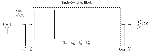
Figure 8: How MDS calculates S-parameters
and Gamma values.
In the prime reference system, the transducer gain equation is
now
In a 50 ohm system, Gamma_s' = 0 and Gamma_L' =
0. Equation (2) then reduces to GT' = |S21'|2.
Surprisingly, GT' is equal to GT
(refer to your lecture notes for an explanation of why this is
so). In this section, you will examine the transducer gain versus
frequency relationship using both equation (1) and (2).
Computing GT using equation (1)
In this approach, the overall amplifier circuit is broken down
into three separate test circuits - IMN, BJT, and OMN. S-parameters
and reflection coefficients are computed as a function of frequency
for each test circuit separately, and the resulting values are
used in equation (1) to find GT.
EQ1: How to find Gamma_s vs frequency
- The circuit required to find Gamma_s versus the frequency
is identical to the circuit in Figure 5. Hence, you have already
collected the necessary data (S-parameters from 0.9 GHz
to 1.1 GHz). The Gamma_s vs f data are stored in
the DS_IMN dataset.
EQ1: How to find the BJT S-parameters vs frequency
- The circuit required to find the BJT S-parameters versus
the frequency is identical to the one used to characterize the
BJT. Therefore, you have already collected the necessary data.
The S-parameter vs f data are stored in the DS_BJT
dataset.
EQ1: How to find Gamma_L vs frequency
- The circuit required to find Gamma_L versus the frequency
is identical to the circuit in Figure 6. Hence, you have already
collected the necessary data (S-parameters from 0.9 GHz
to 1.1 GHz). The Gamma_L vs f data are stored in
the DS_OMN dataset.
EQ1: How to find GT vs frequency
Now that you have all the necessary data, how do you extract the
required values to compute GT using equation
(1)? In addition to evaluating equations on a circuit page, MDS
also has the capability of defining equations on a display page
(i.e., a presentation page). You can create new variables from
scratch, or you can access data (such as S-parameters)
that are stored in different simulation datasets. Of course, you
can also perform standard mathematical operations on the variables.
s11x=DS_BJT.sim1.SP.S[1,1]
s12x=DS_BJT.sim1.SP.S[1,2]
s21x=DS_BJT.sim1.SP.S[2,1]
s22x=DS_BJT.sim1.SP.S[2,2]
Gamma_S=DS_IMN.sim1.SP.S[2,2]
Gamma_L=DS_OMN.sim1.SP.S[1,1]
Gamma_IN=s11x+((s12x*s21x*Gamma_L)/(1-s22x*Gamma_L))
G1=(1-(mag(Gamma_S))^2)/(mag(1-Gamma_IN*Gamma_S))^2
G2=(mag(s21x))^2
G3=(1-(mag(Gamma_L))^2)/(mag(1-s22x*Gamma_L))^2
GT=G1*G2*G3
GT_dB=10*log(GT)
Figure 9: Equations for calculating GT
Figure 9 shows the equations that you need to enter on the presentation
page. The variable names s11, s12, s21, and
s22 are reserved in MDS, so you have to use slightly different
names. Unlike equations on a circuit page, there is no special
EQUATION statement that precedes equations on a presentation
page.
Notice the syntax for assigning data from a dataset to a variable
name. For example, the variable s11x accesses a data array
(S[1,1]) of type S-parameter (SP) from simulation 1 (sim1)
within an external dataset (DS_BJT). It is important to realize
that the defined variables do not contain just a single value,
but an entire array of values (one value for each frequency tested).
MDS performs mathematical operations on variables on an element-by-element
basis. Therefore, the variable GT_dB is an array that contains
the computed transducer gain at each tested frequency.
To add the equations in Figure 9 to a presentation page, follow
this procedure:
- Click [SUI:Presentation] to create a blank presentation page.
Call the new page GT_vs_f.
- Choose [MB:INSERT/EQUATION/FROM DATASET]. The 'Dataset variable
viewer' dialog window appears.
In the input box next to the label Variables in dataset:,
type the name of the dataset you want to access. For example,
to define the equation for s11x, you would type DS_BJT
in the input box. In the input box next to the label Equation
name:, type the name of the variable you wish to define (such
as s11x). In the lower panel
of the window, click the button next to the data parameter within
the dataset that you want to retrieve (such as S[1,1]).
When you are done choosing, click [OK]. An outline of the equation
tags along with the mouse pointer. Position the pointer on the
presentation page where you want the equation to go and click
the mouse button to drop the equation onto the page. Repeat this
procedure for each equation listed in Figure 9.
TIP: It is fairly tedious using the equation dialog window.
It is actually faster to select an equation, copy it to the clipboard
(use [MB:COPY/TO CLIPBOARD]), insert the copy onto the presentation
page (use [MB:INSERT/FROM CLIPBOARD), and then directly edit the
copy to achieve the desired result.
- Once all of the equations have been entered onto the presentation
page, add two listing columns to the page by using [MB:INSERT/LISTING
COLUMN]. Edit the header of the first listing column to show the
frequency (use the DS_BJT dataset). Change the header of the second
listing column to "GT_dB", which is the equation variable
you defined earlier. Assuming your data and equations are correct,
the listings should clearly indicate the variation of GT
(in dB) with frequency.
EQ1: Items to turn in
- Submit a printout of the presentation page which contains
the GT equations and the GT_dB versus
frequency listings.
EQ1: Questions
- What is the transducer gain GT at the design
frequency? How does GT vary with frequency?
- Does the computed value for GT equal GT,max
(to within a few percent) at 1 GHz?
Computing GT' using equation (2)
For this approach, you use the S-parameter values of the
overall circuit in conjunction with equation (2) to compute .
As a reminder, GT' = |S21'|2.
EQ2: How to find G'T vs frequency
- This correct circuit to simulate is the one shown in Figure
4, with the IMN, OMN, and bias subcircuits in their proper positions.
- Find the overall circuit's S-parameters from 0.9 GHz
to 1.1 GHz in 10 MHz steps. Remember to define the equation variable
s21ms_dB as an output variable.
- Create a new presentation page and add listing columns for
the frequency and s21ms_dB.
EQ2: Items to turn in
- Submit a printout of the presentation page which contains
the s21ms_dB versus frequency listings.
EQ2: Questions
- What is the value of GT' at the design frequency?
- Does the computed value for GT' equal GT,max
(to within a few percent) at 1 GHz?
- From your simulations, does the value of GT'
(computed from eqn (2)) equal the value of GT
(computed from eqn (1)) at each frequency?
Amplifier Circuit 2: Designing for Gp
Assignment
In this part of the lab, you need to re-design your microstrip
matching networks to obtain a specific operating power gain (Gp)
at the design frequency. The requirements are a) Gp
= 16 dB, b) magnitude of Gamma_L is minimized, and c) GT
= Gp.
Circuit construction
- In the Lab3 workbench, create
a new circuit page called Amp_Gp.
The basic amplifier circuit is similar to the one used to test
GT,max, except you should use your re-designed
matching networks. Keep the equation statements that define s21ms
and s21ms_dB and make sure your IMN and OMN are well-tuned.
Circuit layout
- Create a circuit layout for your re-designed circuit. Call
the new layout Amp_Gp.
Items to turn in
- Include the by-hand Smith charts and constant gain circle
chart that you used to re-design the microstrip matching networks.
Briefly explain the reasoning behind your design. List the major
equations you used.
- Turn in printouts of the Gp test circuit
and subcircuits. Submit a printout of the final circuit layout.
Amplifier Circuit 2: Using MDS to verify GT
= Gp
Finding GT
- Determine the S-parameters of the overall Amp_Gp
circuit. Linearly sweep the frequency from 0.9 to 1.1 GHz in 10
MHz steps. Define the equation variable s21ms_dB as an
output variable.
- Once the simulation is done, create a tabular listing of the
S-parameters versus the frequency. In this situation, S[1,1],
S[1,2], S[2,1], and S[2,2] are S11',
S12', S21',
and S22', respectively. Add another
listing column for s21ms_dB (remember that GT'
= |S21'|2 and GT
= GT').
Items to turn in
- Submit a printout of the S-parameter tabular listing
and the s21ms_dB listing.
How to find Gp at the design frequency
Figure 10: Gp test circuit
Figure 10 is the schematic used to determine Gp.
Notice that the IMN circuit is not included in the overall
circuit. The equation for the operating power gain is:
In a 50 ohm system, Gamma_L' = 0. This means equation (3)
reduces to the simpler expression:
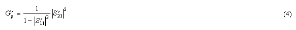
Using an argument similar to the one that proves GT
= GT', it also turns out that Gp
= Gp'.
- Create a new test circuit that corresponds to the schematic
in Figure 10 (use S-ports for the source and load impedances).
If you want to, just modify the Amp_Gp
circuit by omitting the IMN subcircuit. You should add equations
to the circuit page to calculate Gp'. For consistency,
use the equation variable name Gpp_dB for the calculated
value Gp' in decibels.
- Linearly sweep the frequency from 0.9 to 1.1 GHz in 10 MHz
steps. Define the equation variable Gpp_dB as an output
variable.
- Once the simulation is done, create a new presentation page
with listing columns for the frequency and Gpp_dB.
Items to turn in
- Turn in a printout of the circuit you used to find Gp'.
- Submit a printout of the Gpp_dB versus frequency listing.
Questions
- At a frequency of 1 GHz, does the computed value for Gp
meet the design requirement of 16 dB (to within 1%)?
- Does GT = Gp at the design
frequency? Compare the values of GT and GP
as the frequency moves away from the design value. What is the
reason for this behavior?
- How do the input SWR (defined as (1+|S11'|)/(1-|S11'|))
and the output SWR (defined as (1+|S22'|)/(1-|S22'|))
of the overall Amp_Gp circuit vary
with frequency?
Constant Gain Circles
Assignment
You will examine the effect of frequency on constant gain circles.
The test circuit consists of the BJT, two S-ports, and no matching
or bias networks.
Circuit construction
- In the Lab3 workbench, create
a new circuit page called BJT_CGC.
Figure 11 shows what your completed circuit should like. There
are no EQUATION statements.
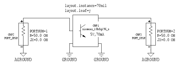
Figure 11: Constant gain circle test circuit
Circuit layout
- You do not have to perform a layout for this circuit.
Simulation
- Do a standard S-parameter simulation. Set Sweep
type="Linear", Start=0.9 GHz, Stop=1.1
GHz, and Step-size=50 MHz. This defines five specific frequencies
for constant gain circle computations. Change the dataset name
to DS_BJT_CGC.
Output
- Click [SUI:Presentation] and create a new display page called
BJT_CGC. Change the Dataset=DATASET
line to Dataset=DS_BJT_CGC.
- Instead of creating a Z-Smith chart the standard way, choose
[MB:INSERT/PLOT/Z-SMITH]. Next, define a rectangular area on the
display page where the chart should be drawn. To do this, click
and drag the mouse from the upper left corner to the lower right
corner of the rectangular area. When you release the mouse button,
MDS will draw a blank Z-Smith chart inside the area you just defined.
- To draw constant gain circles on the blank Z-Smith chart,
you first have to insert a power gain circle equation on the display
page. Choose [MB:INSERT/EQUATION/CIRCLES/POWER GAIN]. An outline
of the equation tags along with the mouse pointer. Position the
pointer outside the frame that surrounds the Z-Smith chart and
click the mouse button to drop the equation onto the display page.
Note that this only defines the gain circle setup conditions but
does not actually draw the circles on the chart (that is a separate
step).
The equation you see on the display page is G=Gcircle(S).
The full syntax of the power gain circle equation is G=Gcircle(S{,StartValue,StepSize,NumCircles,PointsPerCircle}),
where the braces indicate optional parameters. S is the
two-port S-parameter data. StartValue is the initial
power gain (dB) to compute. StepSize indicates the interval
(dB) between successive gain circles. NumCircles tells
how many gain circles to compute. PointsPerCircle determines
the number of evaluated points per circle. The computed gain circle
data is stored in G.
For example, if G=Gcircle(S, 12.5, 0.5, 3), MDS would compute
data for three constant gain circles (12.5 dB, 13.0 dB, and 13.5
dB).
- Click inside the G=Gcircle(S) equation to edit it.
Change the equation to G=Gcircle(S, 15, 0, 1). This tells
MDS to compute a single 15 dB constant gain circle. Since only
one circle is requested, the step size is not important, but it
still needs to be defined.
- Choose [MB:INSERT/TRACE ON PLOT]. The 'Messages' window asks
you to select a plot for inserting the trace. Select the blank
Z-Smith chart with the mouse.
- The 'Expression Error' dialog window appears. In the input
box, type G[*,1,*] and press
RETURN (or click [OK]). MDS now draws a set of constant gain circles
on the Z-Smith chart.
What did that cryptic expression do? G has the syntax G[FrequencyIndex,
CircleIndex, Angle]. The first parameter determines which
frequency to plot gain circles for (* = include all frequencies
in the frequency sweep). The second parameter indicates which
of the computed gain circles to plot at a given frequency (* =
include all circles). The third parameter determines the angle
on the circle for plotting a data point (* = include all angles,
i.e., a full circle).
Hence, the combination of G=Gcircle(S, 15, 0, 1) and G[*,1,*]
causes MDS to draw five separate 15 dB constant gain circles on
the Z-Smith chart, one circle for each frequency in the sweep
from 0.9 to 1.1 GHz . If you had specified G[3,1,*] in
the input box, MDS would only draw the 15 dB circle for the third
frequency index (i.e., at 1 GHz).
Items to turn in
- Submit the Z-Smith chart containing the plot of constant gain
circles versus the frequency.
Questions
- What is the behavior of the gain circles as the frequency
increases?
- The G=Gcircle(S, 15, 0, 1) equation called for a 15
dB gain circle. What happens to the gain circles on the Z-Smith
chart if you try 16 dB? What is the reason for this effect?