EE431/531 Microwave Circuit Design
I: Lab 2
© B. Pejcinovic, P. Wong, O. Woywode
Introduction
This lab concentrates on the principles of designing
impedance matching networks using Smith charts and CAD tools.
You will implement both ell and microstrip circuits to match a
given load to a specific line impedance. In addition, you will
gain experience with MDS techniques such as subcircuits, parameter
sweeps, and optimization.
Although impedance matching networks may seem mundane,
their proper design and implementation is critical to the efficient
transfer of power along the signal path of an amplifier. If there
is an impedance mismatch, electrical signals will undergo reflections
at the boundary of the impedance discontinuity, which can cause
a significant power loss.
Design Specifications
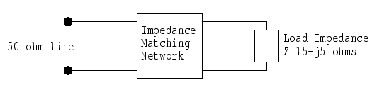
Figure 1: Block
diagram of the matching network
Figure 1 shows the basic layout of the circuit you
are to design. There is a load impedance ZL
that is to be matched to a line with characteristic impedance
Z0. The large block in the center of the figure
will be replaced by your matching network (either ell or microstrip).
The initial values are Z0 = 50
ohm, ZL = 15 - j5 ohm, and the design
frequency is f = 1 GHz.
From the equation Gamma = (z - 1) / (z + 1), where
z = Z / Z0 , the reflection coefficient
of the load is Gamma_L = 0.5423 | -167.5 degrees.
In the actual circuit, the 50 ohm line is represented
by an S-port with a port impedance of R = 50 OH. The 15
- j5 ohm load impedance is approximated by using a 15 ohm
resistor and a 31.83 pF capacitor (which has a reactance of approximately
-j5 ohm at 1 GHz).
You may be wondering what happens at frequencies
other than the design value of 1 GHz. Of course, the capacitor's
reactance will change as the frequency changes, so your matching
network is unlikely to maintain a perfect impedance match at off-frequencies.
However, this is not as unrealistic as you may think, because
real transistor amplifiers have S-parameters that can vary widely
with frequency, which greatly affects the performance of an attached
impedance matching network.
Subcircuits and Miscellaneous Notes
Subcircuit procedure
For simple circuits with few components, it is often
best to construct the entire schematic on a single circuit page.
As the schematic grows larger in size and complexity, it is more
efficient to divide the single circuit into a set of smaller,
modular subcircuits that are reusable. Each subcircuit can then
be tested individually before being assembled into a master circuit.
The process of creating and using subcircuits is
quite easy in MDS. A subcircuit is constructed in almost exactly
the same manner as a standard circuit, except for a few additional
details:
- Construct the subcircuit on a new circuit page.
- Identify and mark the input and output terminals
of the subcircuit.
- Create a symbol for the subcircuit. (Every circuit
page has an associated symbol page, which defines the on-screen
symbol that MDS uses to represent the subcircuit. Although a standard
circuit also has a symbol page, the symbol is usually not defined.
Subcircuits, however, require the symbol to be defined explicitly.)
- Repeat steps 1 through 3 for each subcircuit.
- Construct the master circuit on a new circuit
page. Insert the symbol for each subcircuit into its appropriate
position within the master circuit.
You will implement your matching networks (both ell
and microstrip) as subcircuits. The master circuit consists of
S-ports and the load impedance.
Although the circuits for this lab assignment could
easily be built on a single circuit page, you are asked to use
the subcircuit method for practice.
Miscellaneous Notes
The notation developed in Lab 1 is used extensively
here. Refer to the Lab 1 handout for more information.
Ell Matching Networks
Assignment
You are to design two different ell
circuits (i.e., inductors and capacitors in an "ell"
configuration) to match the 15 - j5 ohm load to the 50
ohm line at an operating frequency of 1 GHz. You have to test
both ell matching networks to examine their performance at various
frequencies.
You may use any combination of inductors and capacitors
that will produce a valid impedance match between the line and
the load. The simplest design method is to use ZY-Smith chart
paper for your initial computations. Since you will turn in your
design charts, carefully annotate them with pertinent information.
Subcircuit construction
- Close all windows that may still be open from
your last lab session. Open the MW_Labs
project file (or whatever your project file is called) by double-clicking
its icon on the main MDS window.
- Create a new workbench called Lab2
within the MW_Labs
project file.
- Create another new workbench called ELL
within the Lab2
workbench.
- Within the ELL
workbench, create a new circuit page called MN_LC1.
This circuit is the first of your two ell matching networks and
should be implemented as a subcircuit.
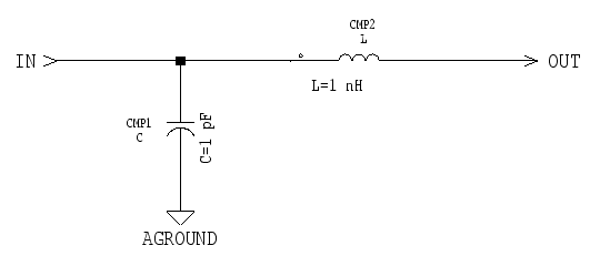
Figure 2: An ell
matching network configured as a subcircuit
- Figure 2 is an example of what the ell subcircuit
might look like (use your own configuration and component values).
Notice that the input terminal ("IN") and output terminal
("OUT") of the subcircuit are clearly identified. The
analog ground is a common node for both the input and output ports
of the subcircuit.
- Build the core of your matching network using
the inductor, capacitor, analog ground, and wire icons in the
Components Palette. If the icons are not visible, click [More
parts …] on the Components Palette, scroll through the 'Parts'
list window, and choose the "Lumped passive" option.
If you wish, you can also directly insert these components by
using the menu bar's INSERT menu.
Next, click [More parts …] and choose the "Connectors"
option from the 'Parts' list. Select the Components Palette icon
that has the floating label Connector in. Use the mouse
to place the input marker at the input node of the matching network.
You may have to rotate the marker to position it properly. In
the blue box next to the input marker, type IN
to identify the input terminal (you can type any text you want,
but descriptive text is usually better).
Select the Components Palette icon that has the floating label
Connector out. Place the output marker at the output node
of the matching network. Type OUT
in the output marker's blue box.
- Make sure 'MN_LC1: CIRCUIT PAGE 1' is the active
window. Choose [MB:WINDOW/CHANGE PAGE/SYMBOL 2]. The original
circuit page is now replaced by its associated symbol page. Don't
worry, your schematic is safe and unaltered. The symbol page is
initially blank except for a dot grid and a cross in the center
of the page. This means that no symbol has been defined yet.
- Select [MB:PERFORM/CREATE SYMBOL]. This automatically
creates a default symbol (a box with numbered and labeled input/output
terminals) and places the symbol in the middle of the symbol page.
Select [MB:INSERT/REF-NAME-LABEL]. A block containing three labels
tags along with the mouse pointer. Place the block underneath
the box symbol and click the mouse button to drop the block onto
the symbol page. MDS uses these labels to uniquely identify the
subcircuit.
Figure 3 is an example symbol page for the subcircuit.
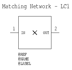
Figure 3: The
subcircuit's associated symbol page
- The optional text above the box was put there
by choosing [MB:INSERT/TEXT], clicking the mouse at the desired
starting position on the symbol page, typing Matching
Network - LC1, and then pressing the
ESC key to finish input. You can change the color of the text
by selecting the text with the mouse and then choosing [MB:SET/COLOR
SELECTED/???], where ??? is one of the defined MDS colors (such
as RED).
When you insert the subcircuit in the master circuit, the subcircuit
will look exactly like the symbol defined on the symbol page.
The default box is quite dull, so MDS includes a number of drawing
tools you can use to create better looking symbols. For the time
being, just leave the symbol as it is (unless you are feeling
very artistic).
- Change back to the circuit page by choosing [MB:WINDOW/CHANGE
PAGE/CIRCUIT 1]. Your subcircuit is now complete! Close the 'MN_LC1:
CIRCUIT PAGE 1' window.
"No load" test case
The load impedance is initially omitted and replaced
by an S-port for S[2,2] measurements. You can then observe what
the load would "see" as the impedance at the output
node of the matching network.
Test circuit construction
- Create a new circuit page called Test_No_Load1
within the ELL
workbench.
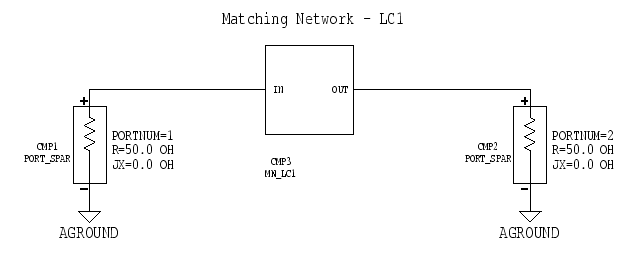
Figure 4: Master
circuit for testing the ell matching network subcircuit with no
load impedance
- The Test_No_Load1
circuit you need to build looks like Figure 4.
- Place S-ports (R = 50.0 OH, JX
= 0.0 OH) on the circuit page using the usual techniques.
Choose [MB:INSERT/COMPONENT/BY LABEL]. A dialog window pops up
that asks you for the label of the design icon to be used as a
component. What this is really asking for is the name of the subcircuit
you want to place on the circuit page. Type MN_LC1
in the input box and press RETURN (or click [OK]).
An outline of the box symbol for your subcircuit tags along with
the mouse pointer. Position the symbol where you want it to go
and click the mouse button to drop it onto the circuit page. You
might have to rotate the symbol to get the proper orientation.
MDS adds the name of your subcircuit to its [MB:INSERT/COMPONENT]
menu for quick access.
Insert analog grounds and connect the various components with
wire.
Simulation
- Click [CIRCUIT:Simulation] to activate the 'Simulation
Setup' dialog window.
- Set the simulation conditions to Type="S-parameter",
Sweep Type="Linear", Start=800 MHz, Stop=1200
MHz, and Step-size=10 MHz.
- Change the default dataset name from DATASET
to DS_Test_No_Load1.
You can do this by clicking [More] on the 'Simulation Setup' dialog
window, clicking [Set host/dataset names …], and entering
the new name in the pop-up input box.
- Start the simulation. MDS will compute the S-parameters
for your test circuit and ell subcircuit.
Output
- Create a new display page called Test_No_Load1.
In the upper left corner of the display page, change the line
that says Dataset=DATASET to Dataset=DS_Test_No_Load1.
- Click [PRESENTATION:Plot] to activate the 'Plot'
dialog window. Click [Select Data …] to open the Dataset
Browser. Choose "DS_Test_No_Load1" as the dataset and
"S[2,2]" as the output variable. Click [OK] to exit
the browser. Set Plot Format to "Z-SMITH" in
the 'Plot' window. Click [OK] to have MDS draw the plot.
- Click [PRESENTATION:Listing] to activate the
'Listing" dialog window. Open the Dataset Browser. Choose
"DS_Test_No_Load1" for the dataset and "freq (Independent
1)" from the Variables list. Click [OK] to exit. Change
Function to "None" in the 'Listing' window. Click
[OK] to have MDS output a column of frequencies on the same page
as the Z-Smith plot.
- Repeat the listing procedure, but this time choose
"S[2,2]" as the output variable. MDS will place the
column of S[2,2] values next to the frequency column.
- The default data format for S[2,2] is to show
real and imaginary parts, which is not very convenient. Click
inside the frame that surrounds the column of S[2,2] values. This
selects and highlights the column. Choose [MB:SET/LISTING COLUMN/DATA
FORMAT/LIN MAG AND PHASE]. This changes the default data format
to magnitude and phase (degrees).
Results to turn in
Note: Remember, you need
to repeat the same construction, simulation, and output procedures
for your second ell matching network. It is highly recommended
that you give the second matching network its own, separate test
circuit. Just follow this procedure:
Close the 'Test_No_Load1: CIRCUIT PAGE 1' window.
In the ELL
workbench, select the Test_No_Load1
circuit icon. Choose [MB:COPY/AS GROUP]. Click and drag the selected
icon to another part of the workbench window to create a copy
of the original test circuit. Rename the copied icon to Test_No_Load2.
You can now open and edit the copied test circuit to use the second
matching network. Change the dataset name to DS_Test_No_Load2
before running the simulation. You can also copy the original
display page and edit it to use the new dataset name.
- Include the by-hand Smith charts that you used
to design the two ell matching networks. Explain how you computed
the required L and C component values.
- Turn in printouts of both ell subcircuits,
as well as a printout of the "no load" master test circuit
(either ell subcircuit is fine; just choose one).
- Turn in printouts of the combined Z-Smith plot
and S[2,2] versus frequency listing for both ell matching
networks.
- Briefly answer these questions:
- S[2,2] is the reflection coefficient at Port
2 when all other ports are properly terminated. Recall that the
load impedance has an equivalent reflection coefficient of Gamma_L
= 0.5423 | -167.5 degrees. How well did your ell networks
match the load impedance at the design frequency?
- As the frequency varies, how does S[2,2] change?
How will this affect the impedance match at frequencies other
than the design value?
- Do both of your ell networks perform equally
as well, or does one do better than the other? Can you think of
practical reasons to prefer one ell configuration over another?
"With load" test case
For this case, the load impedance is placed at the
output of the matching network. Only one S-port is used in the
simulation. You will track S[1,1] to verify the effectiveness
of your matching networks.
Test circuit construction
- Close all open circuit pages and display pages.
Make the ELL
workbench the active window.
- Within the ELL
workbench, create a new circuit page called Test_With_Load1.
This will be a different master test circuit that includes the
load impedance.
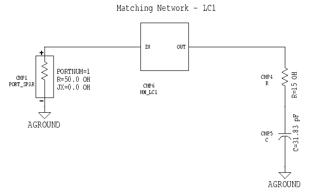
Figure 5: Master
circuit for testing the ell matching network subcircuit with a
load impedance
- The Test_With_Load1
circuit you need to build looks like Figure 5.
- Insert an S-port and the necessary load impedance
components to build the new test circuit. Use the procedures from
the previous section to insert your first ell subcircuit into
the master circuit.
Simulation
- Activate the 'Simulation Setup' dialog window.
The simulation parameters are the same as for the "no load"
master test circuit. Change the default dataset name to DS_Test_With_Load1.
Start the simulation.
Output
- Create a new display page called Test_With_Load1.
In the upper left corner of the display page, change the line
that says Dataset=DATASET to Dataset=DS_Test_With_Load1.
- Create a Z-Smith plot of S[1,1] on the new display
page.
- Add two listing columns to the Z-Smith plot.
One should be the frequency, while the other should be the S[1,1]
values. If necessary, change the data format of the S[1,1] column
to show linear magnitude and phase.
Results to turn in
Note: Remember, you need
to repeat the same construction, simulation, and output procedures
for your second ell matching network.
- Turn in a printout of the "with load"
master test circuit (either ell subcircuit is fine; just choose
one).
- Turn in printouts of the combined Z-Smith plot
and S[1,1] versus frequency listing for both ell matching
networks.
- Briefly answer these questions:
- S[1,1] is the reflection coefficient at Port
1 when all other ports are properly terminated. For a perfect
impedance match, the magnitude of S[1,1] should be zero. Using
this performance measure, how effective are your ell networks
in matching the load impedance to the 50 ohm line at the design
frequency?
- As the frequency varies, how does S[1,1] change?
Microstrip Matching Networks - Part I
Assignment
You are to design a microstrip circuit to match the
15 - j5 ohm load to the 50 ohm line at an operating frequency
of 1 GHz. For the given load impedance, use balanced open-circuited
stubs and a series transmission line.
The substrate is Duroid, with a relative permittivity
of 2.23 and a height h of 0.7874 mm. You may assume that
the microstrip has zero effective thickness.
Use standard Smith chart paper for your initial computations.
Since you will turn in your design chart, carefully label it to
show how you derived your microstrip values. For consistency,
you should express your physical line lengths in either millimeters
or centimeters.
You need to manually compute the microstrip line
width for a 50 ohm characteristic impedance with a Duroid substrate.
Later on you can use the built-in MDS microstrip calculator to
confirm your work.
Subcircuit construction
- Close all open windows except for the Lab2
workbench.
- Create a new workbench called Microstrip
within the Lab2
workbench.
- In the Microstrip
workbench, create a new circuit page called MN_Microstrip.
This circuit page will contain your microstrip matching network
and should be implemented as a subcircuit.
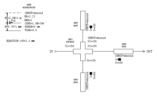
Figure 6: A microstrip
matching network set up as a subcircuit
- Figure 6 is an example of what your microstrip
network might look like (use your own design values). The input
terminal ("IN") and output terminal ("OUT")
of the subcircuit are identified and marked.
Notice how the open-circuited shunt stubs (MSOC - terminal on
one end only) and transmission line (MSTL - terminals on both
ends) attach to the central cross junction (MSCROSS). There is
also a substrate definition block (MSSUBSTRATE) and an EQUATION
statement on the circuit page.
- To access the microstrip components, click [More
parts …] on the Components Palette. Scroll down the 'Parts'
list window and select the "Microstrip lines & bends"
option. The Components Palette now has icons for substrate definition,
transmission lines, and open-circuited stubs. Place these components
on the circuit page.
To access the cross junction component, select "Microstrip
misc." from the 'Parts' window. The icon for the cross junction
will now be available. You may need to rotate some of the microstrip
components to get the proper orientation.
Use wire to connect the various components together. Note that
in real life, the stubs and transmission line coming off the cross
junction are physically joined to the cross as a single microstrip
unit.
Remember to add the Connector in and Connector out
markers to the input and output nodes of the subcircuit.
- Write down the component number (CMP#)
of the transmission line (MSTL) component. You will need to refer
to this number later in the lab.
- Edit the parameters in the substrate block to
have the values show in Figure 6. Add an EQUATION statement to
define the constant w50. This constant should be set to
your computed value for the width of a 50 ohm microstrip line
when the substrate is Duroid. For example, if the computed width
is 2.4 mm, then use EQUATION w50=2.4 mm.
- You can use the built-in MDS microstrip calculator
to automatically compute parameters like the physical line width.
Once the substrate block has been defined, select any one
of the microstrip components on the circuit page by clicking on
it (the transmission line component is a good choice).
Choose [MB:TOOLS/LINE CALC]. The first time you call up the microstrip
calculator, the 'LineCalc Setup' window pops up to allow you to
change the model used for the calculations. The "MSTL"
model is the default choice, so just click [OK]. After a few seconds,
the 'LineCalc Microstrip Transmission Line' dialog window pops
up.
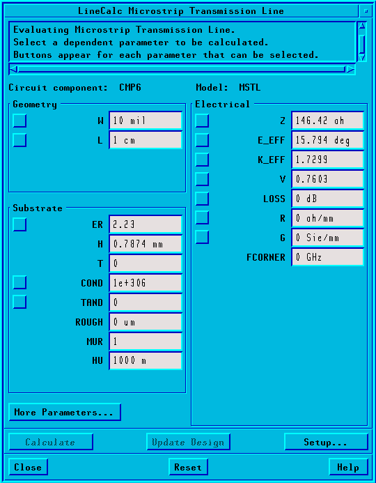
Screen Capture 1:
LineCalc dialog window
- At the top of the dialog window is a scrollable
message area. On the left half of the window are two panel areas.
The upper one is for the geometry parameters (W and L),
while the lower one lists the current substrate parameters. On
the window's right half is a panel area that lists various electrical
parameters of the microstrip line (including the characteristic
impedance Z).
The default unit for the line width is mils. If you prefer some
other unit (like mm), edit the input box next to the W
label. Change the unit from mils to your preference. You can ignore
whatever value may be currently in the input box.
Look at the message area. It should be asking you to select a
dependent parameter to be calculated. Click the button next to
the W label. The message area should now be asking you
to select an independent parameter. Edit the input box next to
the Z label. Change the value there to the characteristic
impedance you want (50 OH, for example).
Click [Calculate]. The input box next to the W label will
now contain the computed microstrip line width. The value of Z
will also be recomputed, so do not be surprised if the characteristic
impedance value is slightly different from before. Does your manually
computed line width agree with the MDS microstrip calculator?
When you are done, close the microstrip calculator window. If
MDS asks if you want to update your microstrip component with
the newly computed value, answer "No".
- Each microstrip component has a SUBST
parameter, which should be set to "duroid" since that
is what is defined in the substrate definition block. The W
parameter is the physical (not electrical) width of the microstrip
line. Set all the W parameters (including W1 through
W4) to "w50", which you have previously defined
in the EQUATION statement. The L parameter is the
physical length of the microstrip line. Set the L parameters
to your design values. Notice that the cross junction has no L
parameter.
- Switch to the symbol page that is associated
with the circuit page. Using the procedures outlined in the ell
section, create a symbol for your microstrip subcircuit (remember
to add the REF-NAME-LABEL block underneath the symbol). When you
are done, switch back to the circuit page and close the circuit
page window.
Test circuit construction
- Create a new circuit page called Test_With_Load
within the Microstrip
workbench.
- Construct a master test circuit that looks like
Figure 5, except use your microstrip subcircuit instead of the
ell subcircuit. When inserting the subcircuit via the [MB:INSERT/COMPONENT/BY
LABEL] command, type MN_Microstrip
when you are asked to enter the label of the design icon to be
used as a component.
- Write down the component number (CMP#)
of the inserted microstrip subcircuit. You will need to refer
to this number later in the lab.
"No optimization" case
You will test the effectiveness of your original
microstrip design prior to optimization.
Simulation
- Activate the 'Simulation Setup' dialog window.
- Configure a standard S-parameter simulation with
a linear frequency sweep from 800 to 1200 MHz in 10 MHz steps.
Change the dataset name to DS_Test_No_Opt
before starting the simulation.
Output
- Create a new display page called Test_No_Opt.
In the upper left corner of the display page, change the line
that says Dataset=DATASET to Dataset=DS_Test_No_Opt.
- Create a Z-Smith plot of S[1,1] on the new display
page.
- Add two listing columns to the Z-Smith plot.
One should be the frequency, while the other should be the S[1,1]
values (in linear magnitude and phase format).
Results to turn in
- Include the by-hand Smith chart that you used
to design the microstrip matching network. Explain how you computed
the required microstrip component values.
- Turn in printouts of the microstrip subcircuit
and the "with load" master test circuit.
- Turn in a printout of the combined Z-Smith plot
and S[1,1] versus frequency listing for the microstrip subcircuit.
- Briefly answer these questions:
- How well did your microstrip matching network
perform at the design frequency? How did the microstrip design
compare to your ell matching networks?
- As the frequency varies, how does S[1,1] change?
- If each stub is made longer by an electrical
length of Lambda/2, what would be the new physical length of each
stub in your design? How would the longer stubs affect the value
of S[1,1] at the design frequency? Compare the S[1,1] - frequency
relationship between a circuit with the longer length stubs versus
a circuit with the original length stubs.
"Parameter sweep" case
You will instruct MDS to sweep the length L
of the transmission line microstrip component to see if the impedance
match can be improved. The lengths of the open-circuited stubs
will be left alone for now.
The subcircuit and master test circuit are unchanged
from the "No optimization" case, so you can re-use them.
On the other hand, you have to make some minor alterations to
the simulation setup for a parameter sweep. If you want to preserve
the setup of the original master test circuit, make a copy of
the test circuit first. You can then work on the copy without
disturbing the original test circuit.
Simulation
- Close all open display page windows and make
the master test circuit page the active window.
- Activate the 'Simulation Setup' dialog window.
- In the 'Simulation Setup' window, change the
Sweep Type to "Single point". The 'Simulation
Setup' window should update itself to show a single input box
next to the Frequency label. Edit the contents of the input
box to set the value "1 GHz". MDS will perform the simulation
only at the design frequency.
- Click [Sweeps/control …]. The 'Sweeps and
Control' list window pops up. From the list of options shown,
choose "Parameter sweep" and click [OK].
Screen Capture 2:
Parameter sweep setup
- The 'Simulation Setup' dialog window changes
its appearance again. On the left side of the window is a new
panel area labeled Simulation sequence that has a list
of selectable options. The list's first option (by default) is
"SWEEP:sweep1", which activates the parameter sweep
setup. The other option is "SP:sim1", which returns
you to the standard 'Simulation Setup' dialog window.
- On the right side of the dialog window is a panel
area for setting the parameter sweep conditions. Remember those
component numbers (CMP#) you were told to write down? You
will need those values now.
For example, if your microstrip subcircuit symbol is CMP8
and your transmission line component is CMP6, then type
cmp8.cmp6.L
in the Parameter name input box. This tells MDS to 1) access
component CMP8 (the microstrip subcircuit) on the master
test circuit page. 2) within the CMP8 subcircuit, access
the component CMP6 (the transmission line), and 3) select
the length L of CMP6 as the parameter to sweep.
Use the component numbers from your own circuit designs.
For future reference, if a circuit component has a parameter that
can be edited, you can tell MDS to sweep the value of that parameter
(as long as it makes sense, like the resistance of a resistor).
- You have to decide on the range of the parameter
sweep. The limits and step-size of a parameter sweep are determined
solely by the range of values and resolution you want to see.
The base unit of the parameter sweep is derived from the component
value's unit on the circuit page. For example, if the transmission
line component has its length specified as L=1.0 cm, then
the base unit is meters and not centimeters. Likewise, if you
specified the length as L=10 mm instead, the base unit
is still meters. (MDS prefers MKS units.)
Suppose L0 is the original length of the transmission
line component. Arbitrarily let x be 25% smaller than L0,
and let y be 25% larger than L0. For
the example case of L=1.0 cm, this means x is 0.75
cm = 7.5 mm = 0.0075 m, and y is 1.25 cm = 12.5 mm = 0.0125
m.
MDS requires that you express the limits and the step-size as
numeric values that are modified by a multiplier of the base unit.
Some of the pre-defined multipliers are "x1.0", "milli",
and "micro", which are used to multiply the numeric
value by 1, 10-3, and 10-6, respectively.
Therefore, you can choose to express x as either "7.5
milli" or even "0.0075 x01". Note that there is
no built-in MDS multiplier for "centi", so you
cannot express x as "0.75 centi".
Now is the time to configure the remaining sweep conditions. Set
Sweep type="Linear". Next to the labels Start,
Stop, and Step-size are input boxes for you to enter
the required values. Adjacent to each input box is a button for
selecting the value multiplier. Just click the button and select
the appropriate multiplier option from the pop-up list.
With this information, set Start=x milli, Stop=y
milli, and Step-size=100 micro. Remember to replace the
x and y limits with your own numbers (expressed
in millimeters).
Under these conditions, MDS will perform a linear sweep of the
transmission line's length L. It will start at x
millimeters and stop at y millimeters. The step size will
be 100 micrometers (0.1 mm).
- Click [More] and change the dataset name to DS_Test_Swp.
Click [Start] to begin the simulation.
Output
- Create a new display page called Test_Swp.
In the upper left corner of the display page, change the line
that says Dataset=DATASET to Dataset=DS_Test_Swp.
- You now need to display the results of your parameter
sweep (which is S[1,1] versus L).
Add a listing column of S[1,1] values (in linear magnitude and
phase format) to the new display page.
Add another listing column next to the S[1,1] column. When in
the Dataset Browser, choose "DS_Test_Swp" as the dataset
and the "cmp8.cmp6.l (Independent 1)" option as the
output variable. Your component numbers may be different. Click
[OK] to exit the browser. In the 'Listing' dialog window, set
Function="None". Click [OK].
Notice that the listing column for the swept L parameter
has units of meters. If there are not enough digits displayed
for the precision you want, select the L column by clicking
inside its frame. Then choose [MB:SET/LISTING COLUMN/DIGITS/4]
to increase the number of digits to four (you can pick any number
of digits you like).
Examine S[1,1] as a function of L. Is there a value of
L that makes the magnitude of S[1,1] closer to zero than
your original transmission line length? If necessary, re-run the
simulation with a wider sweep range to catch the minimum S[1,1]
value.
Results to turn in
- Turn in a printout of the S[1,1] versus transmission
line length L listing for the microstrip subcircuit.
- Briefly answer these questions:
- Were you able to "tune" your microstrip
circuit for better impedance matching performance? At the design
frequency, how large was the magnitude of S[1,1] at the optimum
length L? Compare this to the value you got from the "No
optimization" case.
- How would you go about optimizing other parts
of your microstrip matching network using the parameter sweep
method?
"Full optimization" case
As you may have noticed, parameter sweeps are a powerful
but tedious method for performing circuit optimizations. In this
section of the lab, you will let MDS do almost all the work to
fully optimize your microstrip matching network.
You need to make some fairly radical changes to the
simulation setup for an optimization run, and you also have to
edit the subcircuit. If you want to preserve your original work,
make copies of both the subcircuit and master test circuit first.
Subcircuit changes
- Before MDS can optimize your circuit, you first
have to specify the component parameters in your design that should
be optimized. You then edit the parameter values of those specified
components to conform to a special optimization format. This format
places lower and upper limits on the allowed range of the component's
parameter value. For parameter values that you do not want optimized,
you can just leave them alone.
After all the component parameters that should be optimized have
been properly edited, you next enter the goals (using a special
goal editor) that MDS should achieve during the optimization.
Once the simulation begins, MDS will try to meet the stated goals
by adjusting the specified parameter values within the limits
you imposed.
- You can assume that the microstrip line width
is a fixed value that depends on the characteristic impedance
and the substrate. Hence, MDS only needs to optimize the line
length of each microstrip component.
- Suppose one of your microstrip components has
a length L0. Let x be 25% smaller than
L0, and let y be 15% larger than L0.
The x and y values are the lower and upper limits
that constrain MDS during the optimization. Their exact values
are arbitrary and should be set to the numbers that are most appropriate
for your simulation. The wider the range, the more values MDS
can try during the optimization. Be careful in choosing your limits,
since they can adversely affect the optimization time and the
accuracy of the results. Note that each component parameter may
have its own set of limits that differ from another parameter's
limits.
Change the L=L0 parameter of the component
to L=(x < L0 < y). As a concrete example,
if one of your microstrip components has a length parameter L=1.0
cm, change the parameter to L=(0.75<1.0<1.15) cm.
The initial guess for the optimal solution will be the center
value of 1.0 cm. As the simulation progresses, MDS will adjust
the initial guess between 0.75 cm and 1.15 cm. Note that the number
of digits you use is significant. For instance, a center
value of 1.00 cm is a more precise initial guess than 1.0 cm.
Refer to Figure 7 for an example of what the special optimization
format looks like for a real component.
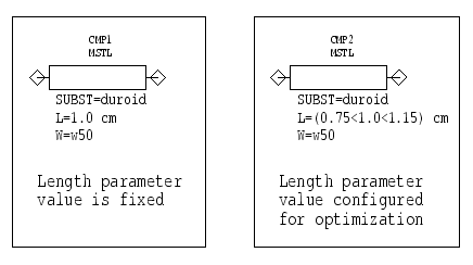
Figure 7: Editing
the parameter value for optimization
- Open the circuit page that contains your microstrip
subcircuit. Edit the L parameters for each of your microstrip
components (the two shunt stubs and the transmission line). When
you are done adding the limit values, close the subcircuit window.
Simulation
- Close any display page window that might still
be open and make the master test circuit page the active window.
- Activate the 'Simulation Setup' dialog window.
- In the 'Simulation Setup' window, set Sweep
type to "Single point" and Frequency to "1
GHz". Actually, you could request a linear frequency sweep,
and MDS would try to optimize your design over the entire frequency
range. To keep things simple, just perform the simulation at the
design frequency.
- Click [Sweeps/control …]. The 'Sweeps and
Control' list window pops up. From the list of options shown,
choose "Optimization" and click [OK].
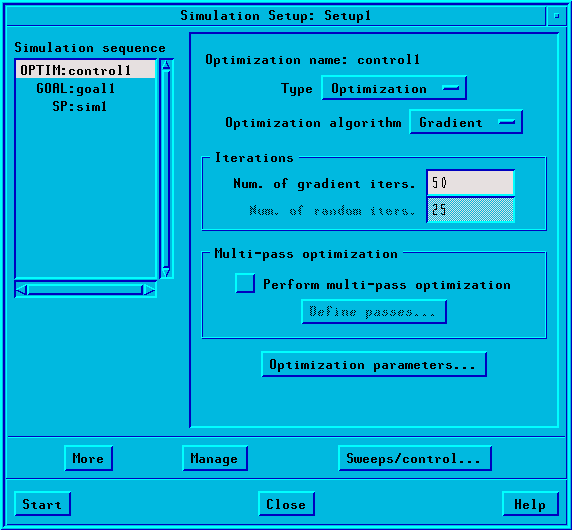
Screen Capture 3:
Optimization setup
- The 'Simulation Setup' dialog window now changes
its appearance. On the left side of the window is the Simulation
sequence list. The list's first option (by default) is "OPTIM:control1",
which activates the optimization setup. The second option is "GOAL:goal1",
which loads the goal editor. The last option is "SP:sim1",
which returns you to the standard 'Simulation Setup' dialog window.
- On the right side of the dialog window is a panel
area for setting the optimization conditions. Set Type
to "Optimization", Optimization Algorithm to
"Gradient", and Num. of gradient iters. to "50".
There are actually three types of algorithms you can choose from.
"Gradient" performs a gradient descent search, which
is best when your component values are nearly optimal already.
It may, however, get stuck in a local minimum and miss better
possibilities. The "Random" option uses random search
techniques, which is appropriate when your initial values are
not very exact. The problem is the random search may leap over
a good minimum that the gradient approach would catch. The final
optimization algorithm is "Hybrid", which combines the
best attributes of the other two algorithms. Unfortunately, the
hybrid approach can be highly time intensive.
- In the Simulation sequence list, select
the "GOAL:goal1" option to call up the goal editor.
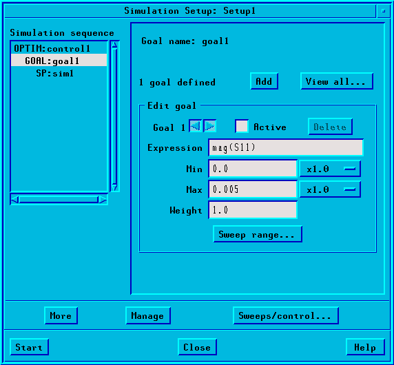
Screen Capture 4:
Goal editor
- The 'Simulation Setup' dialog window changes
its appearance again. The Simulation sequence list is still
on the left half of the dialog window. On the right half of the
window is the goal editor.
In the input box next to the Expression label, type mag(s11).
This tells MDS to track the magnitude of S[1,1] as the goal. Next,
you need to impose constraints on the goal by defining the minimum
(Min) and maximum (Max) allowed goal values.
Next to the labels Min and Max are input boxes for
you to enter the allowed goal values. Adjacent to each input box
is a button for selecting the value multiplier (exactly like a
parameter sweep). Set Min to "0.0" and Max
to "0.005". Use a multiplier of "x1.0". Finally,
set Weight to "1.0".
With the stated goal parameters, MDS will try to optimize the
microstrip component lengths so that the magnitude of S[1,1] is
between 0.0 and 0.005. The weight parameter controls relative
weighting for a multiple-goal optimization and can be ignored
for this single-goal case.
You can change the Min and Max parameters to any
values you want, but be sure what you choose is realizable and
reasonable. If the constraints are too tight, the optimization
process might fail. If the constraints are too loose, MDS will
do a poor optimization job.
For a simple impedance matching network, only one goal is needed.
For bigger projects (such as a multi-stage amplifier), you can
define multiple, simultaneous optimization goals.
- Click [More] and change the dataset name to DS_Test_Opt.
Click [Start] to begin the simulation.
- If you want to monitor the progress of the optimization,
choose [MB:PERFORM/MNS/SHOW PROGRESS]. If for some reason the
optimization process is taking too long, you can abort the simulation
with [MB:PERFORM/MNS/ABORT SIMULATION]. You can also use [MB:PERFORM/MNS/SHOW
ERRORS] to get details on error messages related to the simulation.
These commands are very useful and work with most types of simulations
(not just optimization).
- After the simulation is done, the 'Messages'
window tells you the Cost factor of the optimization, which
is a measure of the error between the stated goals and the actual
results. Lower cost factors are generally better.
- To see the optimal values determined by MDS,
choose [MB:PERFORM/MNS/SHOW BEST VALUES]. The 'Completed optimizations'
window appears, which contains a list of the simulations that
have been performed recently. Click the button next to the simulation
you want and then click [OK]. The 'Messages' window will show
the optimized values of your component parameters.
- Try the [MB:PERFORM/MNS/UPDATE DESIGNS] command.
The 'Completed optimizations' window appears again, so click the
simulation you want and then click [OK]. The 'Messages' window
will inform you that backannotation is completed.
What does this command do for you? Well, MDS takes the optimized
values and inserts them into your circuit page as the new center
values in the edited component parameters. Why is this useful?
If you change the simulation mode back to normal (by clicking
[Sweeps/control …] on the 'Simulation Setup' dialog window
and choosing the "None" option), the center value of
the range is automatically used by MDS as the default component
value. You do not have to change the special optimization format
back to the original fixed format to perform standard simulations.
Note that the number of digits you used for the original center
value will determine the number of digits that MDS uses when it
updates the center value with the optimized value.
Output
- Create a new display page called Test_Opt.
Be sure to set Dataset=DS_Test_Opt.
- Add an S[1,1] listing column (in linear magnitude
and phase format) to the new display page. You should have a single
S[1,1] value in the column (for f = 1 GHz).
Add a new listing column to display the optimal length values
of your microstrip components. In the Dataset Browser, choose
"DS_Test_Opt" as the dataset, "Control1.OPT"
as the package, and "mn_microstrip.cmp2.l" as the output
variable. Your CMP# may be different. Click [OK] to exit
the browser. In the 'Listing' dialog window, set Function="None".
Click [OK]. MDS now outputs the optimal L value for microstrip
component CMP2.
Add new listing columns for the remaining microstrip components.
When you are done, you should have the optimal lengths for both
open-circuited shunt stubs and the transmission line.
- If you are not satisfied with the optimization
results, change the component parameter limits or adjust the goal
constraints and then re-run the simulation.
Results to turn in
- Turn in a printout of the S[1,1] value and optimal
microstrip component lengths.
- Briefly answer these questions:
- How does your optimized S[1,1] value compare
to the original unoptimized value?
- What is the percentage difference between your
original and optimized component lengths?
Microstrip Matching Networks - Part II
Assignment
Design a new microstrip circuit to match the 15 -
j5 ohm load to the 50 ohm line at an operating frequency
of 1 GHz. This time, use a quarter-wave transformer and either
1) balanced open-circuited shunt stubs of length 3*Lambda/8,
or 2) balanced short-circuited shunt stubs of length Lambda/8.
Assume the substrate is Duroid, with the same parameter values
as in Part I.
Choose one of the stub configurations and
compute the physical microstrip line widths and lengths. This
would be a good opportunity to use the MDS microstrip calculator
to simplify your work. Just be sure that the MDS calculator is
using the correct substrate values.
This is a paper design only. You do not have
to construct and simulate your design using MDS, although you
are certainly invited to do so if you want to experimentally verify
your calculations.
Results to turn in
- Turn in all Smith charts (if any) that you use
to design the matching network. Explain how you computed the necessary
microstrip line widths and lengths.
- Sketch what your completed matching network would
look like and label the important parts (quarter-wave transformer,
shunt stub, etc.). Indicate the electrical length, physical length,
and characteristic impedance of each microstrip component.
- If you decide to perform circuit simulations
in MDS, turn in your circuit schematics and plot results.